This speaker started as a spinoff from this thread where I was studying the effects of different levels of stuffing/damping in a TL:
http://www.diyaudio.com/forums/multi-way/281281-pmc-tl-stuffing.html
The speaker that inspired this was the PMC TB-1:
Which has a 48in long internal path TL with the following damping scheme, which I think provides a borderline critically-damped aperiodic TL based on the measurements I have seen on-line:
There was a rather lengthy debate in that thread about whether or not the TB1 follows Bailey's TL approach and whether or not a proper TL should have single or double impedance peak. Rather than debate it, I decided to model it.
I then went on to model and design my own little TL box to study the effect of damping but using drivers I had on-hand: a Dayton Classic Series DC130A-8 5.25in midwoofer and a Dayton DC28F-8 silk dome tweeter. Both of these drivers actually have quite nice published and measured performance specs and are great sounding high-value drivers. You might be hard pressed to find another 5.25in class midwoofer with the same performance for $20. Similarly, the DC28F is an extremely smooth sounding soft dome with low distortion and flat frequency response.
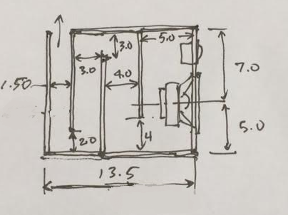
Anyhow, my design constraints were to use approximately the same 48in long TL that the PMC TB-1 has, and about the same physical format. I put the vent in an up-firing position at first, but eventually went with forward firing to gain a few dB of sensitivity in the bass. I also wanted a tuning frequency fb of about 60Hz - 80Hz depending on the damping scheme used.
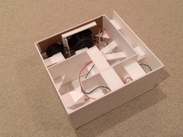
The design of the TL was as follows with a 6.0in wide internal dimension:
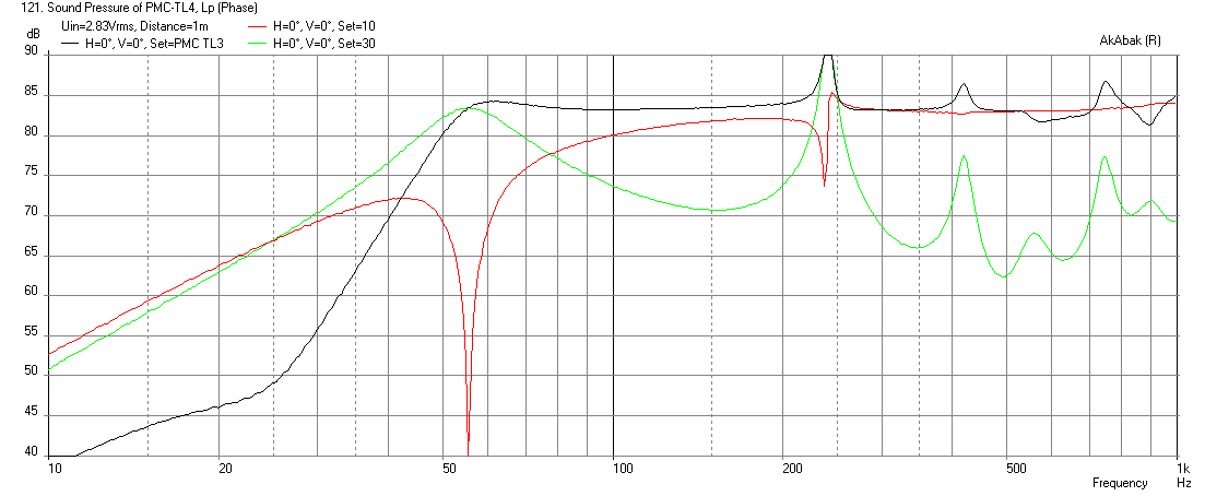
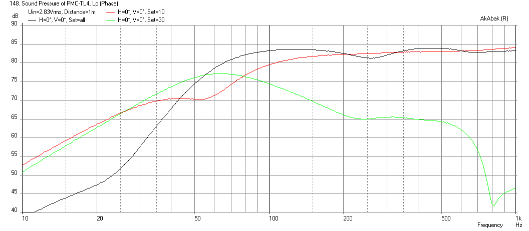
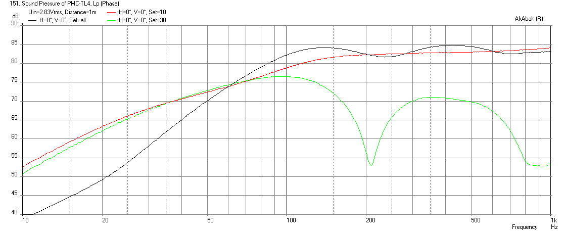
The predicted frequency response for this TL depended heavily on the amount of stuffing inside. Here are 3 cases of light, moderate, and dense stuffing. As expected, each case is a tradeoff in bass extension and SPL for light damping with lower group delay and improved transient response with dense stuffing. The predicted impedance curves go from double peak for light stuffing, to single peak for dense stuffing. The dense case tends to an aperiodic TL.
Light stuffing:
Moderate stuffing:
Dense stuffing:
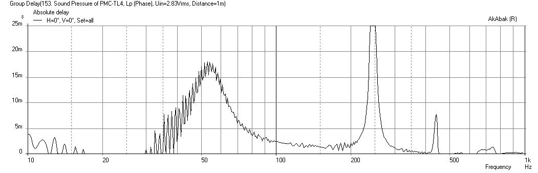
Here are the corresponding Group Delays for the light to dense stuffing, the GD goes from 16ms down to under 5ms at 50Hz which is about the same as a sealed cabinet, but with deeper bass extension.
Light:
Dense:
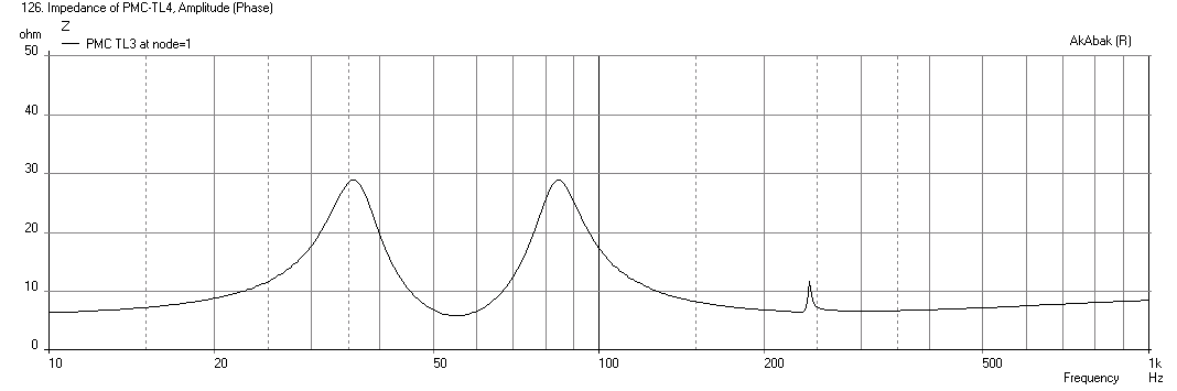
Here is the predicted impedance for light stuffing:
Moderate stuffing:
Dense stuffing:
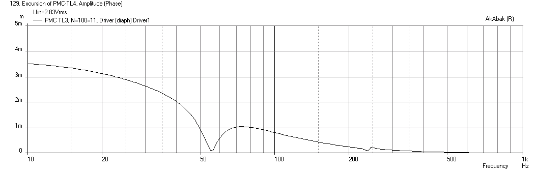
The predicted speaker cone excursion goes from a classic double peak 4th order:
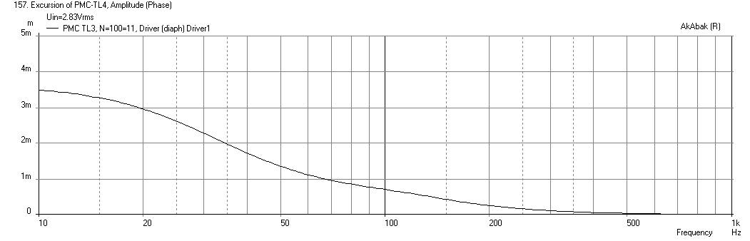
To what you would see in an aperiodic TL or a sealed cabinet:
So these plots intrigued me and I decided to go with a prototype build in foam core. I was aiming for the moderate to dense case somewhere in between. I thought it important to get at least a -3dB point at 80Hz to get a sense of some bass output. I redid the model with front exit vent and the stuffing plan closer to how I will implement it using loosely teased out polyfill. Here is the predicted frequency response with a 2kHz XO and baffle step loses included:
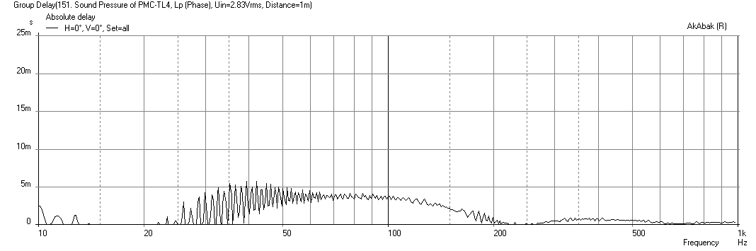
And here is the predicted GD:
If stuffing is added to the final leg, here is the predicted response - about 80Hz f3:
With about 7ms GD at 50Hz:
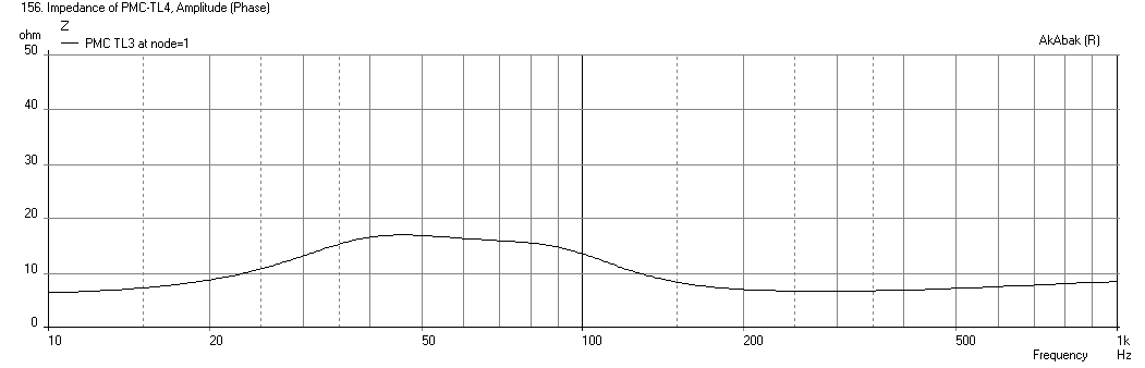
With a semi-bordering on aperiodic TL impedance peak with a mild double bump:
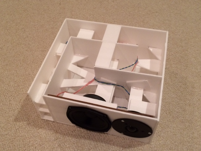
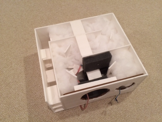
Anyhow that was the goal and here is the build process:
Stuffing plan (adding stuffing in final leg transforms to aperiodic TL):
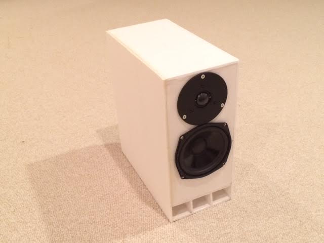
Here is the completed speaker:
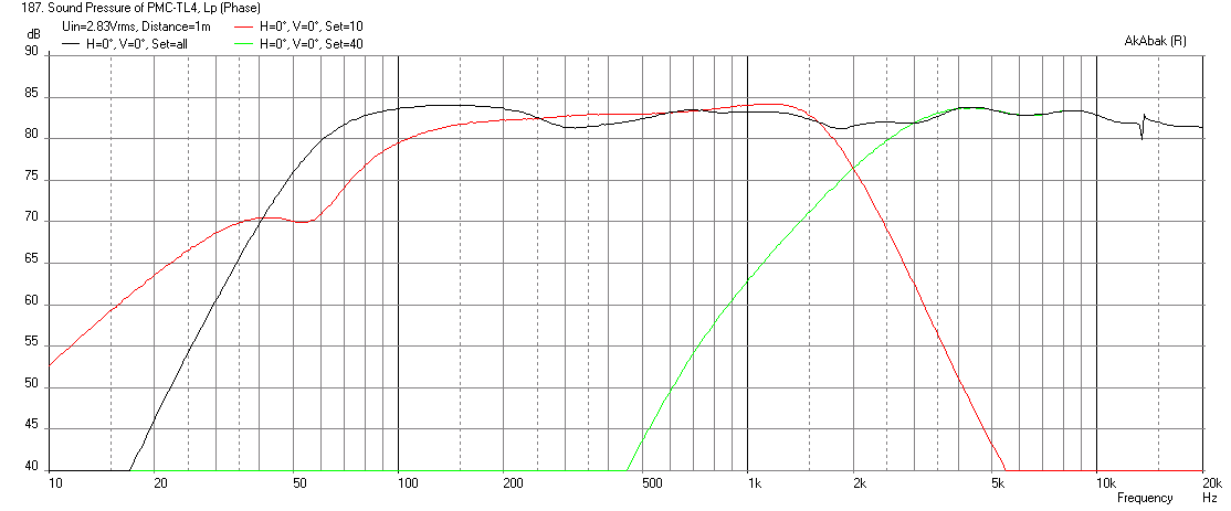
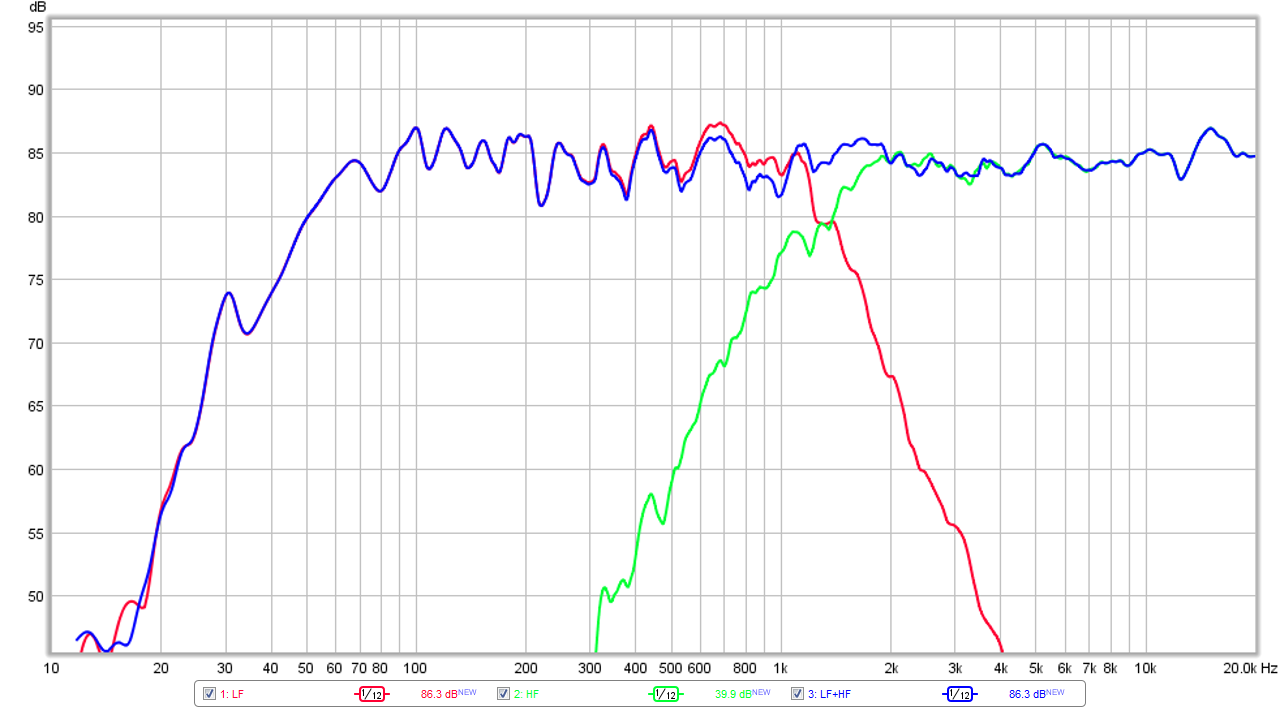
And here are the measurements using a miniDSP and TPA3116D2 amps for an active 2-way. I am using 1st order electrical HPF at 2kHz on the DC28F and a 4th order BW low pass at 1kHz on the DC130A to get an acoustic XO of about 1350Hz. The slopes are quasi-Harsch and allow somewhat of a time-coherent output. I will refine the XO later but these are just to get started.
Raw measurement of the woofer in the TL running full range:
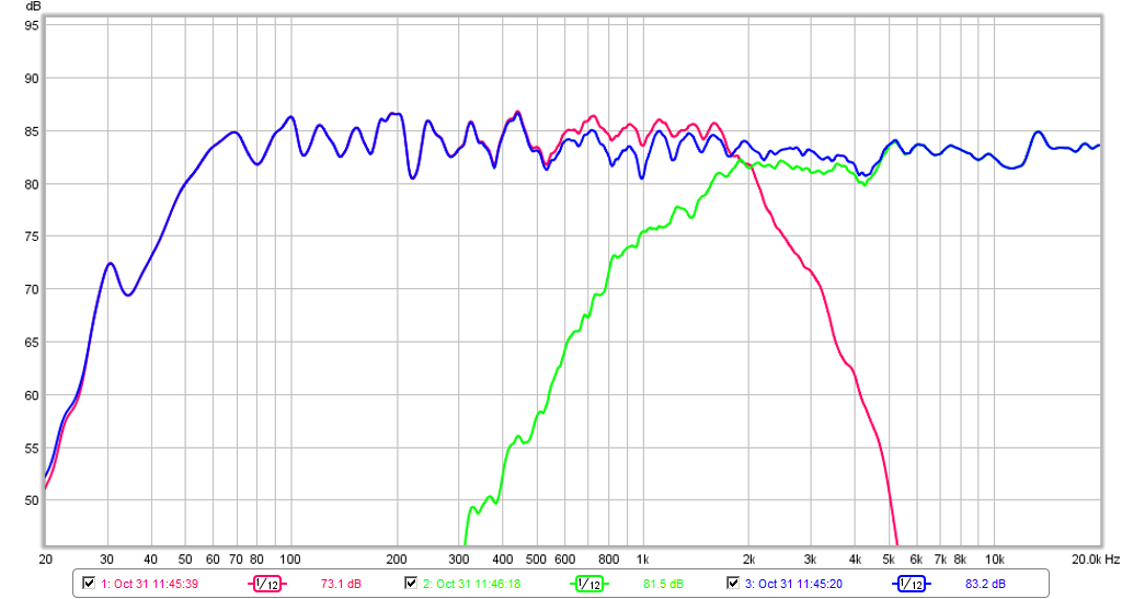
Frequency response showing XO profiles:
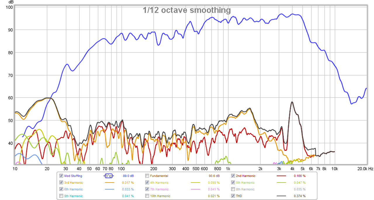
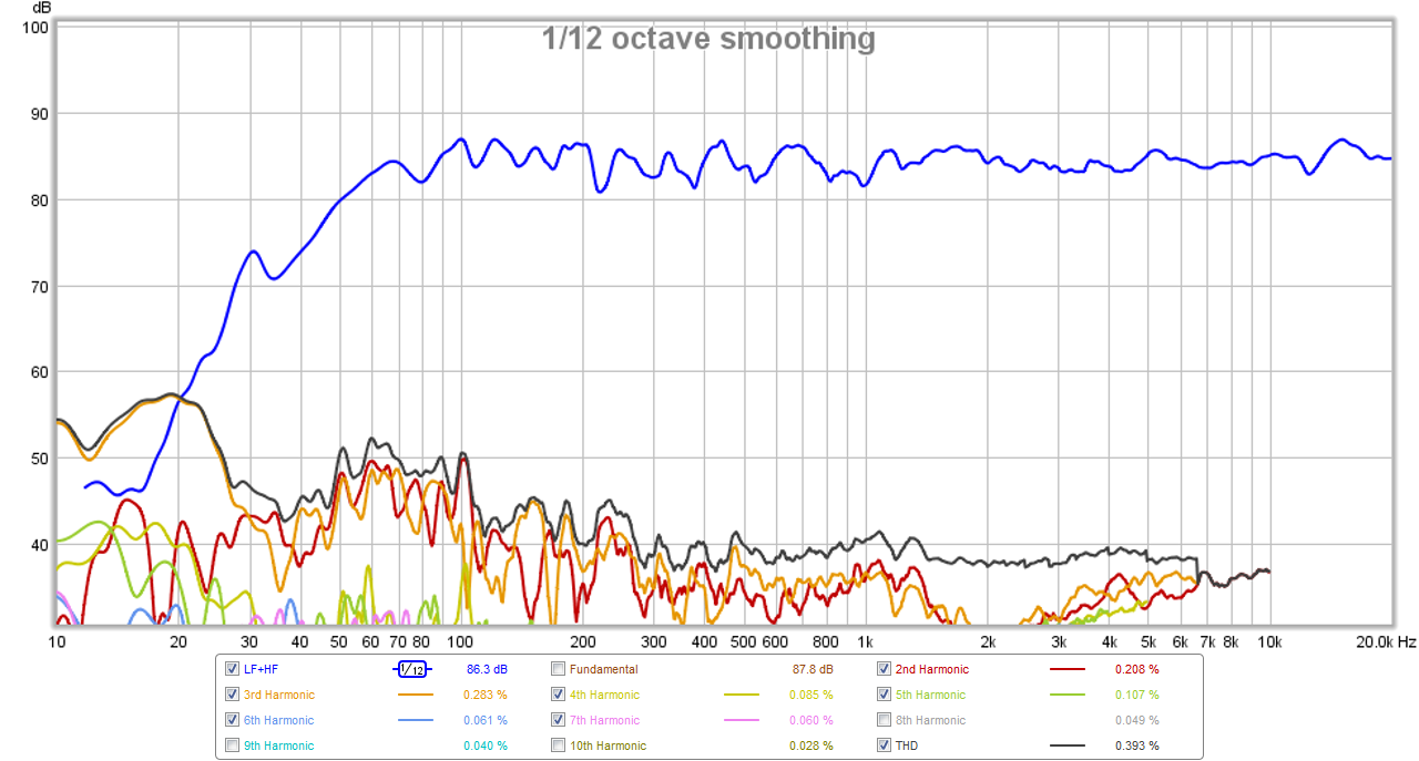
Harmonic Distortion:
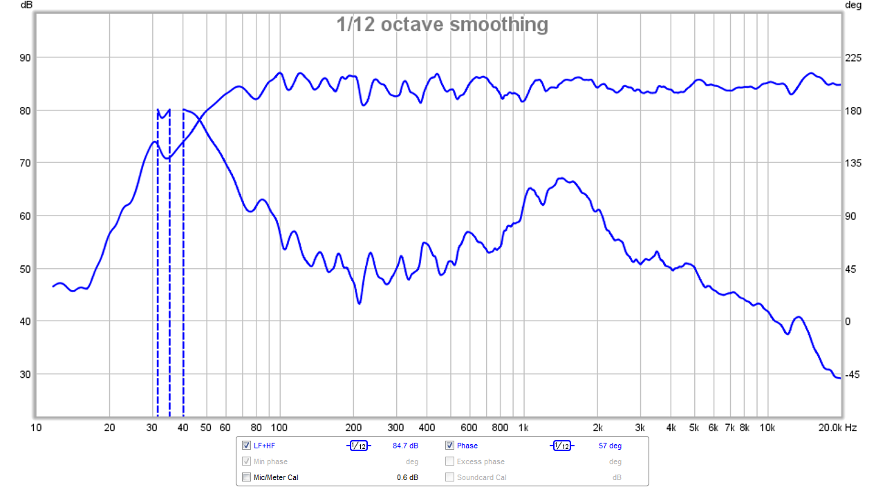
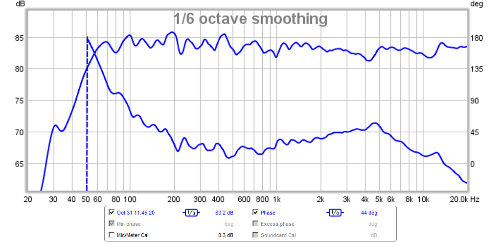
Phase:
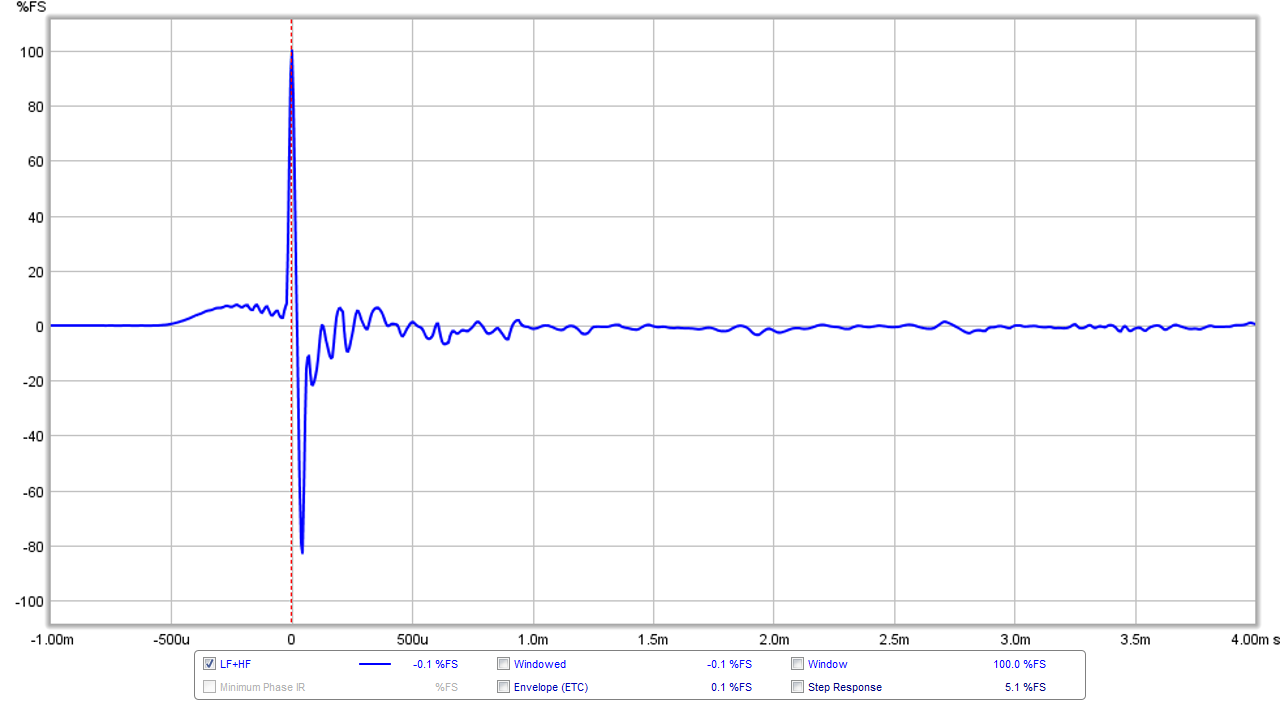
Impulse Response (there is a slight rise and wiggle before the main pulse due to the time delay on the tweeter to get it to be quasi transient perfect with the woofer):
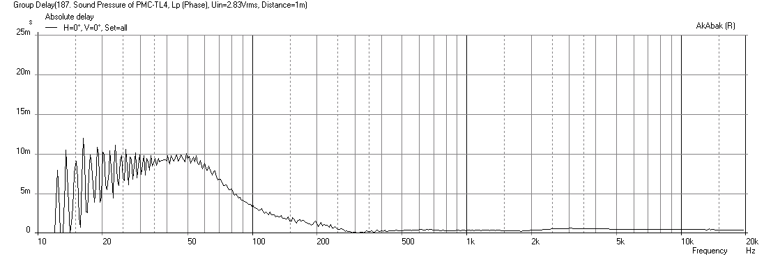
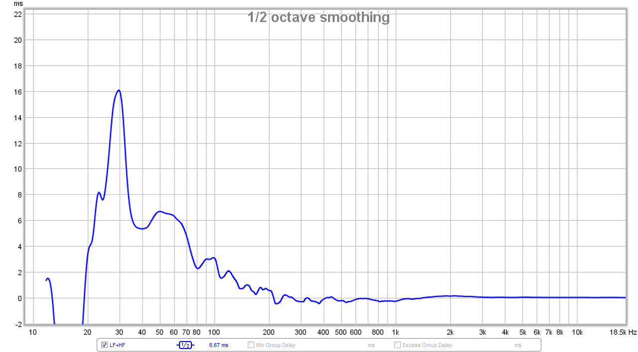
Group Delay (with 1/2oct smoothing for clarity) is about 6.7ms at 50Hz:
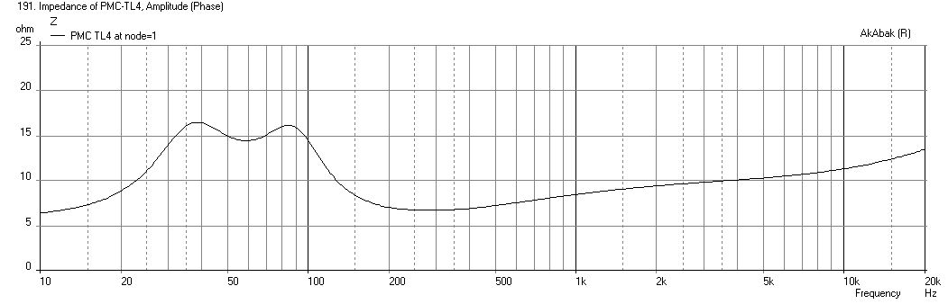
I did take impedance sweeps and they look a lot like the mild double bump prediction above.
The TL sounds very nice - the transients are well aligned in time between the two drivers, the bass is clear and precise without the muddiness of a reflex, the mids are articulate and pleasing, and the highs of the DC28F are excellent - very smooth, transparent, engaging, with no sibillance or harshness. I still need to do more work to refine the XO with careful measurements and simulation in PCD, then transfer to miniDSP rather than doing the XO "by eye". I think I might move the XO up towards the 2kHz point but see that there is additional HD from the woofer there to avoid. If I have time, I may even try to design my first passive XO to see how that looks. Of course it won't be transient perfect given the flush baffle.
I am quite happy with how these turned out and am considering a thin 3/16in Sureply wood baffle to permit the drivers a better mount.
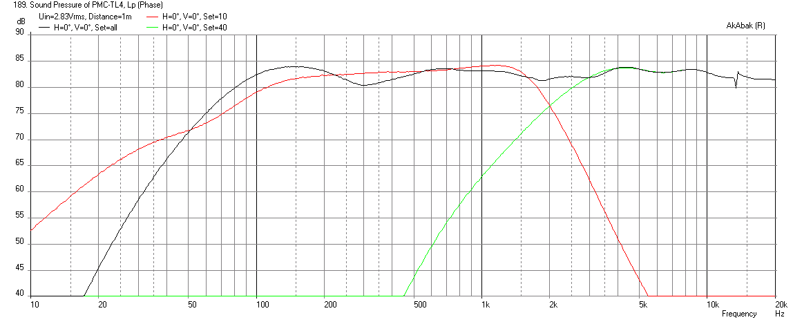
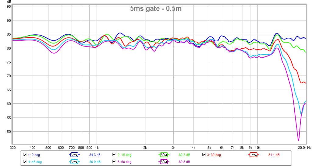
Edit 10/31/15: Polar data shown has tweeter rebated and brillo pad diffraction reducers installed
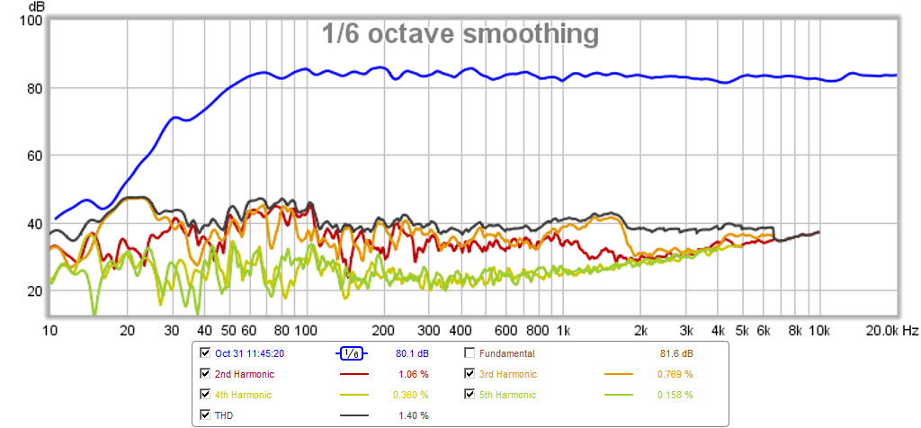
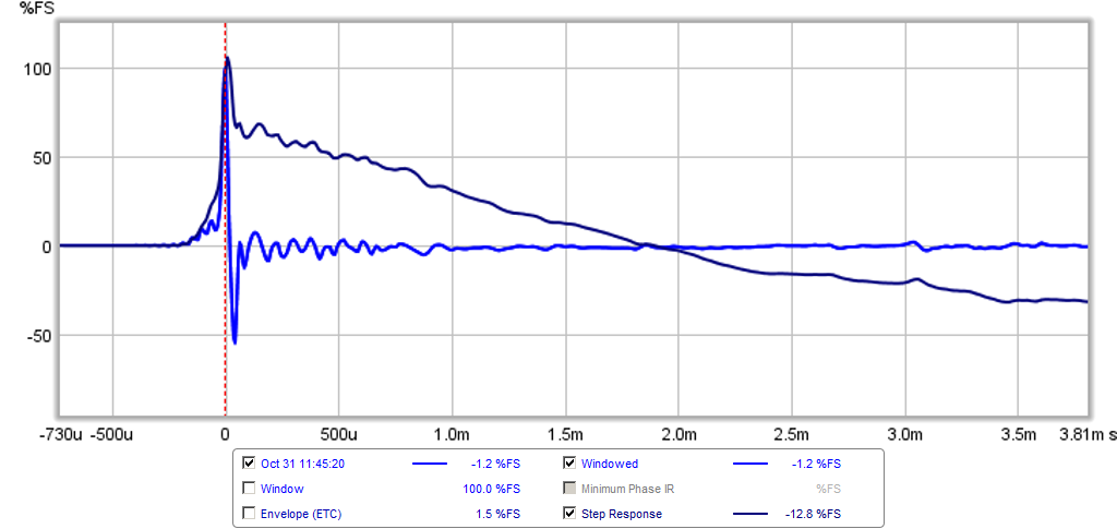
Edit 10/31/15 - latest Measurements with 2kHz XO and rebated tweeter with brillo pad diffraction control - sounds great and settings are now"locked down" for enjoyment (and to build stereo pair):
XO plot:
Phase - +/-23deg over 150Hz to 15kHz :
Harmonic Distortion - about 1.4% at 50Hz at normal listening levels:
Impulse Response/Step Response - very nice:
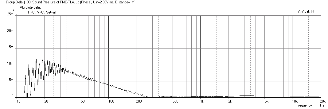
Group Delay (8.6ms at 50Hz - increased 2ms due to BW1 HPF at 32Hz):


