I just made myself a high voltage regulator that I could use for my tube experiments. If you also need a high voltage regulator with good performance, or want to make use of the jellybean parts around, here's a design that is fully simulated and tested.
Features
- Ripple rejection measured at least 93dB (limited by apparatus)
- Output noise measured at most 50μVrms
- Using TL431 as voltage reference and LM317 as pass transistor
- Ability to add soft start function
- No bulky film capacitor needed (if a bit higher noise floor can be tolerated, so the PCB could be made smaller than a credit card!)
Yes, I know there's the
21st Century Maida Regulator, which is very applicable and I even built one myself. But after intense experiment I'd like to share some ways you can tune a regulator better or more suitable to your case. Perhaps I could call this regulator the 2020s Maida Regulator
😉.
Schematic
The good thing about LM317 is that it's available, reliable, and doesn't require a big output capacitor to be stable. However, the
original Maida regulator suffers from poor ripple rejection because of greatly reduced loop gain especially at low frequencies, and the additional 6.9V zener doesn't help much. I found there was a mysterious 1.5Hz voltage fluctuation on my mains and the Maida regulator was almost helpless. (In fact I even tried a 100V zener. It did help a little, but for greatly increased noise and temperature coefficient.)
A TL431 driving LM317 is always seen as a form of super regulator: it has very high ripple rejection, at least
IN THEORY. My regulator uses the same idea but adds protection to every low voltage part so they can regulate a higher voltage. (Q1 protects U1, Q2 protects U2, Q3 protects U3) For details of the components see the following sections.
Measurements
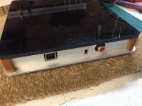
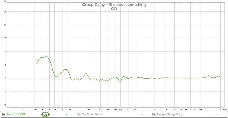
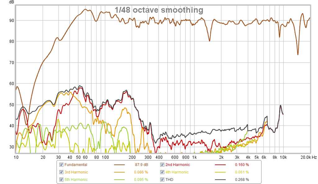
I tested the prototype PCB using my DIY low noise preamplifier whose input noise density is only 1.4nV/√Hz and bandwidth 0.1Hz~100kHz. (with a 10Hz HPF for the following measurements, image 02 below) All measurements use a 10kΩ load at the output unless specified. The output voltage is 451V, which is a bit off from the theoretical 2.495V/1.8k*(1.8k+330k)=460V because I used 5% resistors. However the voltage reading doesn't change when load changes to 3.3kΩ (136mA).
When C1 is 3.8μF of ceramic capacitors, the output noise is 70μVrms. When C1 is a 4.7μF film capacitor, the output noise is 50μVrms. The image 01 shows the noise waveform 1000x amplified.
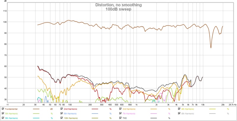
According to the SPICE simulation with the most accurate 431 and 317 model I can find, PSRR reaches 160dB and the output ripple shouldn't exceed 100nVrms. (buried in noise) Reality is mostly disappointing. With an input ripple of 1.8Vrms, the output ripple measured by averaging is 40uVrms which means PSRR=93dB. However my preamp shielding isn't particularly clean and the output might have been polluted by the mains, because measuring the LT3080 version also gives around 45uVrms, which means the majority of output ripple might be mains hum coupled into the scope somewhere. Try measuring it better by yourself to determine the actual PSRR value.
Components
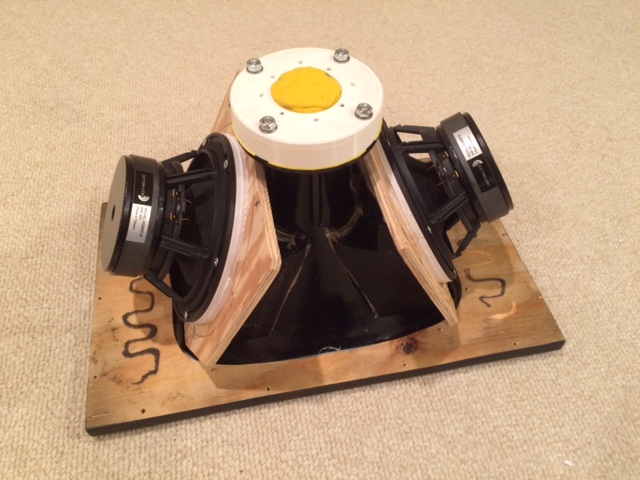
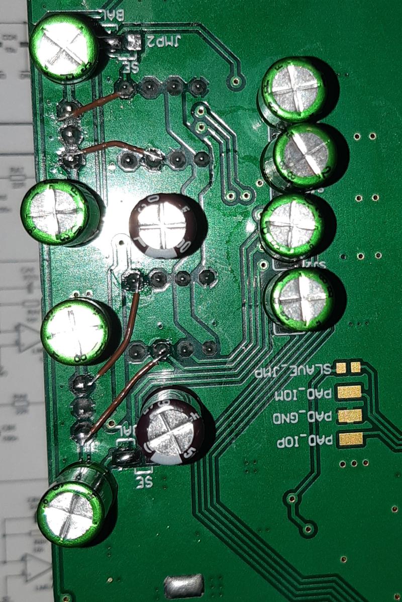
I assembled the prototype board with mainly SMD parts, and ignoring the unused area (which I planned for testing some other circuits) the actual size is smaller than a card. You can use THT parts of course. Here's a list of explanation for some components:
Q2: Power MOSFET used as cascoded U2 protector. I just happened to have STW11NK90Z in hand, but beefier STW12NK95 or lighter STW8NK80Z should also work.
U1: Original Maida regulator uses a Zener diode, but I found using a TL431 gives lower output noise. TL431 has another benefit which is its low output impedance compared to a Zener. This impedance acting with the Ciss of Q2 can create an unwanted pole in the cascode loop, and
may cause parasitic oscillation. See Q1.
Q1: Providing bias current to U1, and isolates the Ciss of Q2 from U1. TL431 typically can only take up to 1nF (for small capacitance) from its cathode, so Q1 also acts as a buffer between U1 and the gate capacitance larger than 1nF. Also if you:
- use a resistor instead of Q1, or
- use two LND150 in series instead of CPC3980, or
- connect Q2's gate to the bottom side of R3 (suggested by The AoE Figure 9.113. To be fair they added a ferrite at the gate.)
then using a 0.5W 15V zener to drive STW11NK90Z will certainly result in oscillation and the HV transformer will shout. Interestingly, 1W zener driving STW11NK90Z (Ciss=3nF) or 0.5W zener driving STW8NK80Z (Ciss=1.32nF) is stable. Meanwhile, I highly suggest that you
DO NOT include a gate stopper resistor for Q2, as it also slows Q2 down and
WILL cause oscillation. These observations are highly component-dependent and I don't know if your parts will behave the same.
U3: Voltage reference and feedback amplifier. This TL431 is protected by Q3, D1, and D4. However, TL431s from different manufacturers
might behave differently. See R10.
Q3: U3 protector by cascoding. I have some LND150 in hand but an enhancement MOSFET with enough voltage rating (like over 600V) should also work. If using an enhancement MOSFET, prepare another bias voltage of around 10 to 15 volts for the gate.
R4: Decrease the thermal dissipation of Q3. If you change the output voltage to be lower this is optional.
R8, R9: Feedback resistor determines the output voltage. Output voltage is 2.495V/R9*(R9+R8)
C1: Adj bypass capacitor for LM317. Can be as low as 0.22uF but the larger C1 is, the lower output noise will be. If C1 is larger than 4.7uF, during start up the output voltage will ramp up for extented period of time. This acts as a soft start. Capacitor larger than 10uF doesn't affect the output noise more but still extends the soft start. C1 also contributes to the loop stability, see R10.
C2: Used for increasing HF loop gain around U3. Maybe be optional but adding it improves PSRR and lowers noise. 0.22uF MLCC is generally enough.
R10: Tunes the HF loop gain. If C1 is larger than around 1.5uF and U3 is a TI or HTC one, then R10 can be 0Ω (shorted). If C1 is smaller, then R10 has to be made larger to ensure stability. For example, when using C1=0.22uF (MLCC), R10 has to be at least 20kΩ. Less R10 results in a noise peaking at higher frequency until the circuit oscillates, but more R10 causes excessive broadband noise at the output, so you might have to trim it for your need. Also, if U3 is from onsemi when C1=3.8uF (MLCC), then R10 has to be at least 10kΩ to be stable. (but the noise rises to 400μVrms, so not a good deal) Again, these are only the results from the batch of parts I have, and your build might behave differently.
All caps used here are rated 600V or higher. They can be polarized ones but polarized capacitor tends to take a lot of place and the value can be too large for this application.
I wish this little application note might offer some help for those who want to build a power supply. Keep safe and good luck.


.jpg")
.jpg")
 But it was quite exciting, with


