Cheers! I am seeking advice and guidance in attempts to restore a piece of analog audio history.
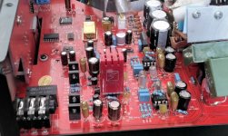
This Mitsubishi DAr10 receiver powers up passing a dim bulb test. However, relays do not click in; there is no sound produced in either channel. The preamp is OK. I can get a signal from the tuner with measurable output on REC OUT. Voltages in the amp circuits resemble what is shown at 'test points' in the SM.
(see attached jpgs. I could not upload the entire SM or copy/paste from the PDF. )
An STK1050 power IC produces output for each channel. Measurements for IC601/left channel were way off. Voltage readings on IC501 seem OK.
Additionally, the DC offset on L601 was in the order of volts! not mV! This could NOT be adjusted by VR601. Looks like the left channel either received a 'blow' or simply failed due to age. I removed the STKs, the impressive heat sink, and decades of domestic detritus. Also purchased new 1050s from SEMITRON on eBay.
I came upon a clever way to trouble shoot an amp circuit like this:
STKs removed, solder 4 resistors of equal value to jump in/out pin pads , gain down, preamp set to aux. My pairs are 1,4 and 0,7. — a Trouble-Shooting Setup…
I was expecting the relays to engage ---no click... suggesting the HA12002 protection IC failed. Replaced it. (I was correct) Now, relays engage and the DC offset on L601 was reduced but still high and unresponsive to turns on the trimmer (VR601).
Taking a closer 'look' at the circuit involved w/DC offset --the N-channel JFET (Q601)-- and the trimmer responsible for adjusting DC offset; desoldered and tested - it is OK. Readings from the gate to R615, 614 did not compare to those on Q501. Since this gate is linked to L601 through C606, R612, R613 I pulled these out- tested OK- reinstalled --Presto! the trimmer now works (very touchy) to zero out the DC on L601.
Must have been a 'cold' or oxidized joint. DC offset now acceptable.
Now, a return to comparing voltages between the two channels raises questions.
(pads 1,4 jumped; pads 0,7 jumped w/470 Ohm resistor)
Readings taken at the power IC terminals:
IC 601 terminals IC 501 terminals
pin 1 -3.5 V -.77 V
pin 2 -42.4 V -42.6 V
pin 4* 0.5 mV -0.2 mV
pin 7* 0.5 mV -0.2 mV
pin 8 ( not included )
pin 9 42.3 V 42.3 V
pin 0 3.48 V .75 V
Pins 3,5,6 not used in this amp design.
*(4,7 measured with Fluke DMM; mV setting w/an averaging function - these voltages tend to wander.)
Questions:
I can infer that there is a DC 'balance' within each channel, but what about between? Why is there that difference between the channels on the #1,#0 pads. Is this a problem? Is this a matter of incorrect idle current/DC bias?
Probing around the transistors with this Trouble-Shooting setup, I find the dc voltages between the two sides comparable until Q504/Q604, Q507/Q607 where a marked difference appears between the values
@the collector of these transistors. The left channel, i.e., Q604/Q607 shows plus & minus 3.47V vs plus/minus .75V on Q504/Q507.
The schematic shows +1.2/-1.2 volts at the #0, #1 points which is the connection to these collectors. Maybe this is only when the STKs are in place. (I recall seeing this 1.2 V before the tear down on the 'good' IC501, right channel).
Here, my novice status becomes apparent.
Does this difference of about 2.75 V matter at all?
I can't explain why, at this drive stage, each side is not producing the same or comparable voltage. Indeed, what is the 'correct' voltage. I don’t see a way to adjust bias. Does this matter?
Testing Results:
A) the protection IC had failed; replaced - relays working
B) reflowing some components around the left channel JFET returned the DC
offset trimmer to 'functional’. DC offset now within specs.
C) the output module, IC601, had failed (via comparative ohms & diode testing) - I have two new STKs in hand
D) a difference of about 2.75V exists between the two sides with regard to DC being presented to the output modules.
Finally.....do you think I should simply install the new STKs at this point ?
Thanks for any feedback/insights.


![20240219_135932[1].jpg](/community/data/attachments/1183/1183519-f54a4d9684ae2c0ae740a8c1a6de8224.jpg?hash=9UpNloSuLA)
![20240219_140642[1].jpg](/community/data/attachments/1183/1183520-f1922ce82faf8883a07e41216b1f85d3.jpg?hash=8ZIs6C-viI)


