Gentlemen, my living-room amplifier (Audio Agile Step AMP, the company "Audio Agile" does no longer exist and I have not been able
to source the amplifiers schematic for repair) passed away 2 month ago, and I need a replacement for it.
I do not like to use my SYMASYM as replacement.
The SYMASYM has been the "working-horse" for all of my projects and works perfectly with them.
Nor do I want and use any of Mr. Nelson Pass' amplifiers.
His amplifiers (I have built his A40, F5, ACA) are too weak (may I therefore call them "CORONA amplifiers" - without being put into the bin?)
to ventilate my speakers (f.e.: KAPPA Infinity 600).
I have remembered Prof. Nelson Pass' amplifier (Release 4.5) to sound very well and have done a layout of my own.
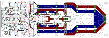
Image1 shows the schematic; Image2 shows the layout.
I have the needed MPSA06, MPSA56, 2N3439 and 2N5416 at hand for 5 pairs of the Leach_AMP PCBs.
I will use NJL0281DG / NJL0302DG with integrated thermal diodes as output transistors.
MOUSER does not currently offer the NJL. But ARROW does!
I have not yet ordered anything from ARROW. Is it a trustworthy company?
If so: I will order 25 pcs. of NJL0281DG/NJL0302DG each and match them (as well as the MPSA transistors) for you.
The PCB size is 228 x 79 mm.
The price for 1 PCB, 6xMPSA06, 5xMPSA56, 2x2N3439 and 2x2N5416 is 15€. A pair of PCBs will then cost 30€ (shipping cost not included).
2 pairs of the Leach AMP PCBs are already spoken for.
Are there any 3 (even more?) of you, who want to build this amplifier?
Give me a PM then.
Best regards - Rudi_Ratlos
to source the amplifiers schematic for repair) passed away 2 month ago, and I need a replacement for it.
I do not like to use my SYMASYM as replacement.
The SYMASYM has been the "working-horse" for all of my projects and works perfectly with them.
Nor do I want and use any of Mr. Nelson Pass' amplifiers.
His amplifiers (I have built his A40, F5, ACA) are too weak (may I therefore call them "CORONA amplifiers" - without being put into the bin?)
to ventilate my speakers (f.e.: KAPPA Infinity 600).
I have remembered Prof. Nelson Pass' amplifier (Release 4.5) to sound very well and have done a layout of my own.
Image1 shows the schematic; Image2 shows the layout.
I have the needed MPSA06, MPSA56, 2N3439 and 2N5416 at hand for 5 pairs of the Leach_AMP PCBs.
I will use NJL0281DG / NJL0302DG with integrated thermal diodes as output transistors.
MOUSER does not currently offer the NJL. But ARROW does!
I have not yet ordered anything from ARROW. Is it a trustworthy company?
If so: I will order 25 pcs. of NJL0281DG/NJL0302DG each and match them (as well as the MPSA transistors) for you.
The PCB size is 228 x 79 mm.
The price for 1 PCB, 6xMPSA06, 5xMPSA56, 2x2N3439 and 2x2N5416 is 15€. A pair of PCBs will then cost 30€ (shipping cost not included).
2 pairs of the Leach AMP PCBs are already spoken for.
Are there any 3 (even more?) of you, who want to build this amplifier?
Give me a PM then.
Best regards - Rudi_Ratlos
Attachments

Last edited:
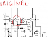
The 10R/2W resistor (R49) at the output makes no sense to me, it seems that it will only serve to increase output impedance and reduce D.F. particular as it is not subject to GNFB... can anyone explain why it is there?
EDIT: A quick search for the original schematic supplied the answer; R49 should be bypassed by an inductor; I suspect made up of enamelled wire wound around the resistor, in practice.
EDIT: A quick search for the original schematic supplied the answer; R49 should be bypassed by an inductor; I suspect made up of enamelled wire wound around the resistor, in practice.
Last edited:
There is an inscription on the PCB - 11 turns, so there will be a coil in parallel. or wound on a resistor.
D.Self writes that the metal parts of the resistor can cause distortion inside the coil. I usually put a coil parallel to resistor.
Well done Rudi,
only those round TO39 heats up, and if you want to put on some round heatsinks - you have to see if there will be space on the PCB and will not interfere with other parts.
i use such similar, only black anodized.
4PCS TO99/TO39 TO-99-39 Aluminum Heat Sinks For OPA627SM LME49720HA OPA128KM | eBay
only those round TO39 heats up, and if you want to put on some round heatsinks - you have to see if there will be space on the PCB and will not interfere with other parts.
i use such similar, only black anodized.
4PCS TO99/TO39 TO-99-39 Aluminum Heat Sinks For OPA627SM LME49720HA OPA128KM | eBay
Whoops, a bit late.
I've never liked the VI limiter. It would benefit from a resistor to the rails, thus giving a two slope action. That means modifying the existiing values, though.
I've never liked the VI limiter. It would benefit from a resistor to the rails, thus giving a two slope action. That means modifying the existiing values, though.
This limiter has never been "turned on" when using this amplifier on a daily basis. As far as I remember the original article - it is designed for low-load protection. at 8 ohms I measured my own Leach amps - 153W in 170W before the clip. 60 an 63V rails.
@Pingrs, osccar:
I have not yet ordered the PCBs.
If you like me to do a change: I will do, in case I approve it.
I like to order the PCBs on this weekend.
Best regards - Rudi_Ratlos
I have not yet ordered the PCBs.
If you like me to do a change: I will do, in case I approve it.
I like to order the PCBs on this weekend.
Best regards - Rudi_Ratlos
no, no - you don't have to make any changes for me. I already have my own Leach amps. These are the little things I'm talking about.
I know this project will run smoothly for you!
I know this project will run smoothly for you!
Rudi:
Check that schematic carefully if you want to build a true Leach amp. There is at least one error!
For example, Leach uses a true emitter follower triple for the output stage; the schematic you showed doesn't.
Best Regards,
mlloyd1
Check that schematic carefully if you want to build a true Leach amp. There is at least one error!
For example, Leach uses a true emitter follower triple for the output stage; the schematic you showed doesn't.
Best Regards,
mlloyd1
...
I have remembered Prof. Leach's amplifier (Release 4.5) to sound very well and have done a layout of my own.
Image1 shows the schematic; Image2 shows the layout.
...
Best regards - Rudi_Ratlos
"I have remembered Prof. Nelson Pass' amplifier (Release 4.5) to sound very well and have done a layout of my own."
A couple (late) recommendations:
Since the power rails VCC & VEE are meant to run very close to +/– 60V, the electrolytic decoupling capacitors should be rated for 100V, not 63V. If lower voltage parts are used, they will have a much shorter lifespan.
In the older amp designs, such as this and the DH-200, -220, the C12 value was only 100 nF. Modern designs use a larger value here, such as 220 uF. The voltage rating on this cap may be 16V.

100V capacitors can be very large ... I think 75 or 80V is enough, look at what is available. seems to be 80V caps usually have 6800 uf or less.
The importance of using sufficient voltage rating for the power decoupling capacitors is such that I would recommend making the PCB larger, if necessary.
Voltage rating is more important than temperature rating (as all are rated to at least 85°C) for electrolytic capacitor lifetime.
Edited to add:
I was originally referring to the smaller 1000 uF capacitors, which can easily be sized for 100V rating. The larger 10,000 uF caps may be more problematic. While 100V would be preferable, 75V or 80V may suffice.
Last edited:
osscar,
Leach uses the T output triple approach that Bart Locanthi developed many
years ago - I recall that he talks about it in his articles. The positive drivers and outputs should ALL be NPN and the negative drivers and outputs should ALL be PNP.
Error is highlighted in the attached schematic snips comparing Leach's original schematic to Rudi's.
There may be other errors; I stopped checking after these.
Best regards,
mlloyd1
output seems to me to be correct ...I don't see any error
Attachments

Ok. Thank you...now i see
Anyway, the Leach amp is what I will always keep.
Low DC offset, no turn on / off thump ... no DC at output if one power rail is lost.
And it sounds good, although of course not eco friendly - 60W idle as I measured. Of course it depends on the type and VA of the transformer and bias current.
Anyway, the Leach amp is what I will always keep.
Low DC offset, no turn on / off thump ... no DC at output if one power rail is lost.
And it sounds good, although of course not eco friendly - 60W idle as I measured. Of course it depends on the type and VA of the transformer and bias current.
Last edited:
@mlloyd1:
Thank you for pointing me to this error.
I have mixed the drivers (MJE15030 / MJE15031) and have changed the schematic / layout accordingly.
I will check the grid of the used capacitors, before I order (on the weekend).
Best regards - Rudi
P.S.: @TungstenAudio: will you please be so kind and give me your opinion?
Attachments

Last edited:
- Home
- Amplifiers
- Solid State
- Professor Leach Amplifier