How can 3/4 plus 3/4 make a wholez?
When two quasi single-ended amplifiers rely on a quarter of the partner. Here is my preliminary finale from the unfortunate thread. It should be noted that the input of the "3/4 + 3/4 = quasi 1 amplifier" would like to be driven with a very low impedance.
HBt.
PS
A test setup will follow.
When two quasi single-ended amplifiers rely on a quarter of the partner. Here is my preliminary finale from the unfortunate thread. It should be noted that the input of the "3/4 + 3/4 = quasi 1 amplifier" would like to be driven with a very low impedance.
HBt.
PS
A test setup will follow.
Attachments


Association!
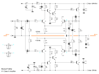
The Musical Fidelity A1 amplifier is often associated with the idea that it is two amplifiers connected in parallel. Dynamically, it is actually a parallel circuit, if you like. Statically, it is two halves. Each half is actually an audio amplifier with an open collector; on the output side, each of the two (complementary) amplifiers is only missing a collector load, a working resistor, a transformer or a suitable current source/sink. So 1 + 1 = 2. Neither a transformer nor a current source or sink are actually present. Nevertheless, the necessary collector load is formed by the mirror image of the other, but now the entire ensemble works in (class A) push-pull.
The decades-long debate as to whether 20W A operation actually exists is completely irrelevant, and the question of the transition to AB operation is also meaningless. There is an A mode, but a slightly different one, because the power consumption of the entire amplifier (compared to the PSU) hardly changes under modulation, it remains constant. Constant up to the limit of the preset maximum load current of a sinusoidal half-oscillation. This is usually 800mA. Above this, an A1 no longer behaves in the same way as a real B or AB representative would due to the topology and dimensioning. This power range should be avoided, or it can be called up for a short time without any problems.
A real 10 watts becomes 20 peak watts, which, as is well known, has often led to the demise of the combined, split output stage. If you want to achieve a maximum of 20W at a static load of 8 ohms, the quiescent current must be increased from 0.8A to 1.12A.
If you like, you could say that the A1 does not supply the required current for the load, the loudspeaker, but subtracts it as a difference from its internal Iq.
Back to the naming “3/4 + 3/4” = 1 + 1/2. Since it is obviously not quite two individual amplifiers (functioning on their own), i.e. neither 1 +1 = 2 nor 1/2 + 1/2 = 1, I tend towards a total and a half. An A1 is just really different.
In addition to the operational reliability and the associated longevity of such a 50°C to 60°C oven, one of the challenges is to reduce the THD somewhat and to eliminate the strange AB behavior as far as possible.
The user @jxdking has another idea for this. Also a very interesting suggestion.
Attachments


Hi @hbtaudio
I might have saved your A1. Right now it is stable.

The feedback network I used is still from the original one. The reason that the original A1 doesn't perform well in Class B region is that C2, C3 above get over charged because of high voltage on the sensing resistors so that the bias current got pinched. The solution is just to remove them.
Regarding the bias current, I take the advantage of the input bias current at the base of LTP transistors. You can adjust feedback network resistor values or the sensing resistors to get the current you desired.
The amp is stable. The miller cap might be oversized (on the safe side). You may use lower values to get more performance.
10KHz, 20Vp into 8 Ohm, -74dB THD, which is on par with Blameless design with 3055/2955.

1KHz, 20Vp into 8 Ohm, -82dB THD

I might have saved your A1. Right now it is stable.
The feedback network I used is still from the original one. The reason that the original A1 doesn't perform well in Class B region is that C2, C3 above get over charged because of high voltage on the sensing resistors so that the bias current got pinched. The solution is just to remove them.
Regarding the bias current, I take the advantage of the input bias current at the base of LTP transistors. You can adjust feedback network resistor values or the sensing resistors to get the current you desired.
The amp is stable. The miller cap might be oversized (on the safe side). You may use lower values to get more performance.
10KHz, 20Vp into 8 Ohm, -74dB THD, which is on par with Blameless design with 3055/2955.
1KHz, 20Vp into 8 Ohm, -82dB THD
Just a quick interrupt - so that the impression is not created that "we only theorize and simulate", no, we put things into practice.
On the photos you can see one of my last A1 ideas, which I had discarded despite being fully functional ... Iq approx. 650mA (sets itself automatically). PSU +/-20Vdc regulated. LTP current source /sink 1.2mA. r_inp = 1k5 -> Inverting function, phase |180°| ... used (at the end) tripple (compound) darlington BC550C+BD140+TIP2955 ... and so on!
It was ten years ago.
Attachments


(...) is that C2, C3 above get over charged because of high voltage on the sensing resistors so that the bias current got pinched. The solution is just to remove them.
Regarding the bias current, I take the advantage of the input bias current at the base of LTP transistors. You can adjust feedback network resistor values or the sensing resistors to get the current you desired.
Perhaps I should (for inspiration only) quickly sketch the schematic for the circuit in the photos from posting #5 ?
For AC signal, you can short C1. 22 Ohm resistor is too small, so that you can ignore it, too. What you get is a bridge, which ensure the AC voltage at Feedback equal to Out voltage. This is pretty clever design.Would you like to write a few words about my red and green circling?
The Red Circle in #6 is used to put offset voltage on the positive inputs, as there is small amount current flowing through the base of the transistor. I believe it is an alternative way to configure output bias current.
Last edited:

👍For AC signal, you can short C1. 22 Ohm resistor is too small, so that you can ignore it, too. What you get is a bridge, which ensure the AC voltage at Feedback equal to Out voltage. This is pretty clever design.
The Red Circle in #6 is used to put offset voltage on the positive inputs, as there is small amount current flowing through the base of the transistor. I believe it is an alternative way to configure output bias current.
It is indeed "a clever design".
Whether Mr. Paravicini was actually the originator of the idea here remains to be seen. It's absolutely not important, it's just advertising.
thx.
And this bridge is loaded with Z(jOmega) = 22Ohm -j 1/(Omega * 10µF) depending on the frequency. However, the two nodes should dynamically follow the corresponding node (or input nodes). They are virtually the same.What you get is a bridge, (...)
T= 22Ohm * 10µF = 220µsec
...
I know 😎No complain for its class A performance. 10KHz, 10Vp into 8Ohm.
But which design are you referring to?
The MF-A1 is seen as a bridge and now we need at least @MarcelvdG for correct analysis of the system.
In fact,
we recognize 1 + 1 = 2 amplifiers, of which each is only 3/4 !
#
I hope that the usual prejudices against the (MF Paravicini) design can soon be dispelled. While Morton kindly continues to work on the design of the opening post - as far as I know.
HBt.
Do we really recognize something similar to a bridge, or rather a classic measuring bridge?

Dear @jxdking,
At the moment I don't understand your wording, what exactly do you mean by: "get over charged" !?
C2 = C3 equal 47µFThe reason that the original A1 doesn't perform well in Class B region is that C2, C3 above get over charged because of high voltage on the sensing resistors so that the bias current got pinched. The solution is just to remove them.
Dear @jxdking,
At the moment I don't understand your wording, what exactly do you mean by: "get over charged" !?
Why don't we solve the offset and Iq problem according to the following pattern ??? Please note that the two offset voltages (or currents) will never be identical in amount.

Let's say the current sensing resistors are 0.47 Ohm at the output stages. The bias is configured that the total voltage drop of 2 resistors is about 1v. Thus, the bias is about 1 A.At the moment I don't understand your wording, what exactly do you mean by: "get over charged" !?
Within the class-A region, the total voltage drop stay the same. Everything is good.
Drive it into class-B, the total voltage of 2 resistors would go beyond the 1v. Because of the existence of the c2, c3 (in #4), they get charged by the higher average voltage from the sensing resistor. The higher the voltage on C2, C3, the lower actual bias point you get. Thus, actual bias point drifts to a low point. At some point, the actual bias point goes into pure class B. That's why it exhibits very high distortion when driven into class B.
Removing C2, C3 doesn't solve the issue completely. C1 is still in the circuit, and it also gets charged up when driven into class B.
Thus, the current sensing feedback approach isn't design for Class AB, B. It only works in class A.
Thanks for your reply, I was afraid you had lost interest in this little amp.
Now we only have to derive the exact A mode (regardless of the apparently set quiescent current). Its limits seem to be related to the way in which the quiescent current is generated.
C1 is still in the circuit, and it also gets charged up when driven into class B.
C1 the small cross-connector, which we always consider simply as an AC short circuit.And this bridge is loaded with Z(jOmega) = 22Ohm -j 1/(Omega * 10µF) depending on the frequency. However, the two nodes should dynamically follow the corresponding node (or input nodes). They are virtually the same.
T= 22Ohm * 10µF = 220µsec
...
Now we only have to derive the exact A mode (regardless of the apparently set quiescent current). Its limits seem to be related to the way in which the quiescent current is generated.
- Home
- Amplifiers
- Solid State
- 3/4 + 3/4 the strange A1