Hallo,
I build these two 555-based 12V to HV.
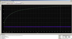
Here the scheme and results.

Added a parallel cap to C4 to reach 33uF.
17.5V to 420V (decreasing of 1V each second since the coil and the IRF740 get warm, hot).
Smell of electronic stuff at high temp.
To avoid fail I just did 1 minute of test.

Added a parallel cap to C4 to reach 33uF.
17.5V to 350V (decreasing of 1V each second since the coil and the IRF740 get warm, hot).
Smell of electronic stuff at high temp.
To avoid fail I just did 1 minute of test.
I just connected multimeter at the output to measure the voltage (load).
What can I do to improve thermal stability and reliability? The coil and the irf get really hot.
I plan to put a heatsink on the irf. But about the coil? Is 3A rated. The design suggest 2.1A coil.
Someone stated that 120uH coil would be a solution.
Im not so skilled and no component at hand to understand or try.
My plan is to achieve a stable 400ish DC voltage to power 4x 12AX7 (6mA?)
Thanks for support Guys
I build these two 555-based 12V to HV.
Here the scheme and results.
Added a parallel cap to C4 to reach 33uF.
17.5V to 420V (decreasing of 1V each second since the coil and the IRF740 get warm, hot).
Smell of electronic stuff at high temp.
To avoid fail I just did 1 minute of test.
Added a parallel cap to C4 to reach 33uF.
17.5V to 350V (decreasing of 1V each second since the coil and the IRF740 get warm, hot).
Smell of electronic stuff at high temp.
To avoid fail I just did 1 minute of test.
I just connected multimeter at the output to measure the voltage (load).
What can I do to improve thermal stability and reliability? The coil and the irf get really hot.
I plan to put a heatsink on the irf. But about the coil? Is 3A rated. The design suggest 2.1A coil.
Someone stated that 120uH coil would be a solution.
Im not so skilled and no component at hand to understand or try.
My plan is to achieve a stable 400ish DC voltage to power 4x 12AX7 (6mA?)
Thanks for support Guys
You may need a different core material.
Also a pull up resistor on the timer.
And a gate resistor with reverse diode on the fet.
Also a pull up resistor on the timer.
And a gate resistor with reverse diode on the fet.
I used to play around with circuits like these years ago.
You need to be sure the drive waveform from the 555 has fast rise and fall times (look with a scope) to avoid the FET operating in its linear region. It must be either fully on or off and nothing in between.
'Everything' depends on getting the frequency correct to suit the coil and the coil must be suited to the load and voltage you are trying to achieve... I can't tell you what values to use before you ask 🙂... but it is all very much interlinked and extremely important. The coil has to be able to 'store' the energy needed in it magnetic core for each cycle.
There have to be better chips than the 555... its a neat idea but its far from optimum. I suspect things get messy trying to implement the feedback for voltage control... messy as in the drive waveform suffers and might become noisy rather than well defined.
You may have to try UC3843 a 8 pin chip.specially made for this application.
Pulse width and dead time built in.
Pulse width and dead time built in.

You'll probably want a Schottky diode for D1. Any reverse charge will be 'eaten' by Q1. You may also want to look at the waveforms around Q1 to make sure the switching waveforms are reasonably clean. Often the switching will excite the parasitics in the circuit, which results in energy loss, thus, heat in Q1.
Note that the output voltage, Vout, for a boost converter is Vout/Vin = 1/(1-D), where D is the duty cycle of Q1's gate signal and Vin is the input voltage. Rearranging:
D = 1-(Vin/Vout). With 12 V input and 200 V output, you're looking at a duty cycle of 0.94 = 94 %.
That high duty cycle will cause the current in the inductor to become quite extreme. You need to make sure the inductor can handle the peak current without saturating. Q1 will need to handle the current also.
Also note that if the input voltage drops, the duty cycle approaches 100 %. That will short circuit the input voltage through L1 and Q1. This will happen every time you turn the circuit off. If the 12 V is from a battery you'll short out the battery every time it reaches 0 % charge. So you need to limit the duty cycle to a value less than 100 % and since the nominal value is 94 % you don't have a lot of wiggle room there.
You would be better off if you started at a higher input voltage, say 48 V. You may also find that a pulse width modulator (which can be based on the LM555 and a comparator) will work better than the 555 by itself. The UC38xx series is excellent. I seem to recall that they offer current mode operation, which can make stability easier.
Tom
Put a small series resistance (0.1) in the source pin.
Watch the waveform on a scope. It should look like a nice triangle. If it looks more like going UP a sky jump the inductor core is saturating. Not good.
The sence resistor peak voltage will tell you the peak current.
With the core saturating only the coil DCR and MOSFET on resistance will limit the on current so current becomes very high.
As "tomchr" pointed out you need some way to limit on time to control max inductor current and stay away from saturation.
"Real" flyback regulators ICs have a sense amplifier to measure drain current and shut down the switch if it comes too high. This is good.
So I also suggest looking at "real" flyback regulator IC.
They are cheep and common and by the time you add all all the functions to make the 555 acceptable I think it will not be a simple circuit any more.
Have a look at the attached data sheet for a UC3845. It will work at a 12V input.
They cost less than a buck, come in dip packages and the data sheet has some circuit examples.
I posted a few app notes. None have exactly your application but you should get the idea.
A application like yours where the output voltage is much higher than the input voltage will required a very short MOSFET on time for a long off time to discharge the inductor at the much higher voltage. That is why I suggested the UC3845 with a 50% max duty cycle although the UC3843 may work fine as well.
However if you wish to see if you can do it with a 555 just for fun, go for it. It will be a adventure at least. I would then as the next step add a comparator to sense max. current and reset the 555 and shut down the MOSFET.
BTW
If you need to get to 400V both the diode and Mosfet voltage rating at 400 volts will not likely be enough. This is because in switching regulators the leakage inductance of the part leads, the connection wires and the storage capacitor will add up to create some over shoot voltage. You need extra part voltage margin to tolerate the over shoot. 50Vs extra is likely marginal, 100V would be my pick if the wiring is short and clean.
Try a MUR160 for the diode for about 50cents.
A snubber is also a possible need to lower the noise level and reduce over shoot. Switchers are fun but not always easy to get noise free.
A pi filter between your switcher and any audio circuit is a good addition.
Attachments
Last edited:
How do you suggest getting from 12 V to the 200 V indicated on the schematic with a maximum duty cycle of 50 %?That is why I suggested the UC3845 with a 50% max duty cycle although the UC3843 may work fine as well.
The maximum boost factor, Vout/Vin would be 1/(1-0.5) = 2 for a maximum duty cycle of 50 %. So you'd be able to get to 24 V. That's not very exciting.
Tom
Your schematic says 200 V. The math gets even worse with 400 V. D = 1-(Vin/Vout), so D = 1-(12/400) = 0.97 or 97 %.My plan is to achieve a stable 400ish DC voltage to power 4x 12AX7 (6mA?)
With the tiny current required, I'd probably look at a flyback converter or a charge pump. A diode-based voltage multiplier could maybe be made to work too.
Tom
Here is a spice sim showing from 12v input for about 475 volts out with a 50% duty cycle and a 66k load @400V (about 6mA).How do you suggest getting from 12 V to the 200 V indicated on the schematic with a maximum duty cycle of 50 %?
With a real regulator it limits the output voltage to 400 voltage at a bit less than a 50% duty cycle.
I picked the UC3845 as it tends to be a little easier to get a stable regulator switch rate in current control systems if the duty cycle is held to less that 50%.
A stable regulator switch rate is important in audio for low noise.
Yes you can also use the UC3843 but will need to be careful to select the circuit values so the inductor is always full discharged before the next switch cycle starts or sub harmonic switching may happen and that tends to be noisy in the audio band.
Attachments

BTW
A better MOSFET would run a lot cooler like a IPAW60R180P7SXKSA1 from Infineon @ about $1.50 each.
The on resistance of the old IRF840 is higher than wanted in this application.
My sim shows a peak inductor current is a bit under 6A. So 3 amp inductor is not great.
Inductor IHLP5050CEER100M01 from Vishay is 10uH at 7 amps with 14 amps saturation current. Cost is under $2. Many others will work.
Last edited:
Ah! You're running it in discontinuous mode. Then the boost ratio becomes:Here is a spice sim showing from 12v input for about 475 volts out
Vout/Vin = (Vin*D^2*T)/(2*L*Iout),
where D is the duty cycle, T is the switching period, and Iout is the output current. That ratio can get pretty large.
It's been a while since I've designed switching converters. Thanks for the opportunity to refresh. 🙂
Tom
Wow Guys! So much material
Thank you all
Im going to make some breadboards to test different situations and compare.
I got the point, is like a multi variable equation with a lot of calculation.
Finally a project where I have to study and really improve my knowledge and skill.
I will update you
Thank you all
Im going to make some breadboards to test different situations and compare.
I got the point, is like a multi variable equation with a lot of calculation.
Finally a project where I have to study and really improve my knowledge and skill.
I will update you
Last edited:
You'll probably want a Schottky diode for D1. Any reverse charge will be 'eaten' by Q1. You may also want to look at the waveforms around Q1 to make sure the switching waveforms are reasonably clean. Often the switching will excite the parasitics in the circuit, which results in energy loss, thus, heat in Q1.
Note that the output voltage, Vout, for a boost converter is Vout/Vin = 1/(1-D), where D is the duty cycle of Q1's gate signal and Vin is the input voltage. Rearranging:
D = 1-(Vin/Vout). With 12 V input and 200 V output, you're looking at a duty cycle of 0.94 = 94 %.
That high duty cycle will cause the current in the inductor to become quite extreme. You need to make sure the inductor can handle the peak current without saturating. Q1 will need to handle the current also.
Also note that if the input voltage drops, the duty cycle approaches 100 %. That will short circuit the input voltage through L1 and Q1. This will happen every time you turn the circuit off. If the 12 V is from a battery you'll short out the battery every time it reaches 0 % charge. So you need to limit the duty cycle to a value less than 100 % and since the nominal value is 94 % you don't have a lot of wiggle room there.
You would be better off if you started at a higher input voltage, say 48 V. You may also find that a pulse width modulator (which can be based on the LM555 and a comparator) will work better than the 555 by itself. The UC38xx series is excellent. I seem to recall that they offer current mode operation, which can make stability easier.
Tom
I include some visual to understand clearly.
Increase the duty cycle increases ON state and so the heating produced.
What about aim a very low duty cycle? Inefficiency I guess, since the output cap needs more time to charge.
Keep a reasonably high duty cycle is important to have a more constant DC output voltage value.
50% remind me half wave rectifier. So a good compromise I guess between stable output, Vinput drop voltage D margin (battery reaches 0%), inductor working and thermal dissipation.
Thanks Tom. 48V is too high. Max 20V.
Since I was working on 555 I would test it at 18V regulated with a schotky diode in series (17.7V). Or 15V regulated, if 555 works bad near the max absolute voltage value of 18V.
Seems that UC38xx is the way to go. Cheap too.
The achieve is a SLO100 PREAMP in a box, pedal box, so I need to run it under 20V
[18V usually or 20V with type-C PD3.0 protocol. OT, why spend lot of money in a multi lane isolated 9v 12v 15v 18v power supply (spyder psu) when you can use a single typeC PD3.0 board per lane with selective voltage? All these type C are connected to a multi typeC PD.30 source (isolated lanes)]
Indeed the switchers are tricky stuff to work with. It's time to use oscilloscope and perform some theory.Put a small series resistance (0.1) in the source pin.
Watch the waveform on a scope. It should look like a nice triangle. If it looks more like going UP a sky jump the inductor core is saturating. Not good.
The sence resistor peak voltage will tell you the peak current.
With the core saturating only the coil DCR and MOSFET on resistance will limit the on current so current becomes very high.
As "tomchr" pointed out you need some way to limit on time to control max inductor current and stay away from saturation.
"Real" flyback regulators ICs have a sense amplifier to measure drain current and shut down the switch if it comes too high. This is good.
So I also suggest looking at "real" flyback regulator IC.
They are cheep and common and by the time you add all all the functions to make the 555 acceptable I think it will not be a simple circuit any more.
Have a look at the attached data sheet for a UC3845. It will work at a 12V input.
They cost less than a buck, come in dip packages and the data sheet has some circuit examples.
I posted a few app notes. None have exactly your application but you should get the idea.
A application like yours where the output voltage is much higher than the input voltage will required a very short MOSFET on time for a long off time to discharge the inductor at the much higher voltage. That is why I suggested the UC3845 with a 50% max duty cycle although the UC3843 may work fine as well.
However if you wish to see if you can do it with a 555 just for fun, go for it. It will be a adventure at least. I would then as the next step add a comparator to sense max. current and reset the 555 and shut down the MOSFET.
BTW
If you need to get to 400V both the diode and Mosfet voltage rating at 400 volts will not likely be enough. This is because in switching regulators the leakage inductance of the part leads, the connection wires and the storage capacitor will add up to create some over shoot voltage. You need extra part voltage margin to tolerate the over shoot. 50Vs extra is likely marginal, 100V would be my pick if the wiring is short and clean.
Try a MUR160 for the diode for about 50cents.
A snubber is also a possible need to lower the noise level and reduce over shoot. Switchers are fun but not always easy to get noise free.
A pi filter between your switcher and any audio circuit is a good addition.
With "real flyback" you mean that UC38xx series? So a chip that is INTENDED (not like 555) to perform what I force to 555 to do with BJT tranny? Thats the flyback right?
About the time of charge/discharge (duty cycle)
So we are aiming to:
- short pulse mosfet ON: high current (12V Vin), inductor charge
- mosfet OFF: high voltage during the discharge of the inductor trought the diode. Energy stored in Output cap.
Q: why the inductor doesn't discharge to the Vin? Im not confident with RLC circuits.
555 is what I found used to similar pedals. But I'm looking for the best cooler (mean thermal) stuff possible.
About the 400V. SLO100 works @360V.
400V+ is something that facinate me to test 12AX7 tubes in harsher conditions. How would be the pleasant distortion?
What you mean for a snubber? A low ohm high watt resistor?
+1 for diode and Thanks buddy
Thanks for scheme. The values at V2 (pulse generator) are what I sould have to produce with UC38xx?Here is a spice sim showing from 12v input for about 475 volts out with a 50% duty cycle and a 66k load @400V (about 6mA).
With a real regulator it limits the output voltage to 400 voltage at a bit less than a 50% duty cycle.
I picked the UC3845 as it tends to be a little easier to get a stable regulator switch rate in current control systems if the duty cycle is held to less that 50%.
A stable regulator switch rate is important in audio for low noise.
Yes you can also use the UC3843 but will need to be careful to select the circuit values so the inductor is always full discharged before the next switch cycle starts or sub harmonic switching may happen and that tends to be noisy in the audio band.
UC3845 has maximum 50% duty cycle: if Vin drop what happens? Does the duty cycle gorw?
UC3843 can go further 50%. So I can decrease the switching frequency and increase the duty cycle?
+1 Better mosfet
+1 bigger inductor
Thanks
This TI appnote will help you to correctly size inductor, switches ( mosfet and diode) and output cap :
https://www.ti.com/lit/an/snva856b/snva856b.pdf?ts=1722706942156
https://www.ti.com/lit/an/snva856b/snva856b.pdf?ts=1722706942156
If you haven't already, I suggest you read up on how boost converters work.Q: why the inductor doesn't discharge to the Vin? Im not confident with RLC circuits.
J.N. Ross, The Essence of Power Electronics would be my place to start. It's a pretty thin book that gives you enough information to get started without drowning you in electromagnetic field theory.
This looks just as helpful as Ross: https://www.monolithicpower.com/en/...electronics/dc-dc-converters/boost-converters
Tom
I can't speak for @Bluesystems but by "real" flyback controller, I'm think he means using an actual SMPS controller IC instead of a 555 timer IC.With "real flyback" you mean that UC38xx series? So a chip that is INTENDED (not like 555) to perform what I force to 555 to do with BJT tranny? Thats the flyback right?
I bristle a bit at the "flyback", though. The UC38xx series can be used for many SMPS converter types, including flyback converters. It'd be every bit as useful in a forward converter, boost, buck, etc.
Nothing prevents you from making your own ramp generator and using it with a comparator to form a pulse width modulator. You can use the 555 as a ramp generator by configuring it as an astable multivibrator. The voltage across the cap that sets the frequency will approximate a ramp. In reality it's two exponentials, but it's close enough to a ramp. Then use a comparator like the LM311 to turn the ramp into a PWM signal.
If you look at the internals of the UC38xx series that's about how they work. They also add current mode control, which is handy. And duty cycle limit for some of them. And the reference voltage that you'll need for the PWM. You get a lot of puzzle pieces in one IC with consistent performance, which is the main selling point.
I made a boost converter in college "a few" years back that used the LM555+LM311 topology described above. The UC38xx wasn't available in the parts store at the college.
Tom
Thanks for theroy material guys. Now I just fast checked the boost topology.
Switch ON: the surge current charge the coil (max A measured to size the coil A, uH sized appropriately to let it charge and discharge in a duty cylce without saturation)
The instant voltage drop acros the coil is proportional to the current change. Our current pass from MAX to 0. So the change must be rapid to achieve high voltage.
I know that a coil opposes at current changes. If I supply constant 1A at 12V, the coil act a conductor with a sort of resistance (very low) after the initial current surge (where it act as insulator).
The coil works with mutual inductance
Switch OFF: the coil now has stored a magnetic field opposite in verse to the current verse.
What I cant get is where this magnetic field discharge.
In this image I resambled the inductor as a capacitor/battery ONLY IN THE MOMENT when it start discharge. Is it a wrong approximation?

Thanks Tom for patience 😉
Switch ON: the surge current charge the coil (max A measured to size the coil A, uH sized appropriately to let it charge and discharge in a duty cylce without saturation)
The instant voltage drop acros the coil is proportional to the current change. Our current pass from MAX to 0. So the change must be rapid to achieve high voltage.
I know that a coil opposes at current changes. If I supply constant 1A at 12V, the coil act a conductor with a sort of resistance (very low) after the initial current surge (where it act as insulator).
The coil works with mutual inductance
Switch OFF: the coil now has stored a magnetic field opposite in verse to the current verse.
What I cant get is where this magnetic field discharge.
In this image I resambled the inductor as a capacitor/battery ONLY IN THE MOMENT when it start discharge. Is it a wrong approximation?
Thanks Tom for patience 😉
WowI can't speak for @Bluesystems but by "real" flyback controller, I'm think he means using an actual SMPS controller IC instead of a 555 timer IC.
I bristle a bit at the "flyback", though. The UC38xx series can be used for many SMPS converter types, including flyback converters. It'd be every bit as useful in a forward converter, boost, buck, etc.
Nothing prevents you from making your own ramp generator and using it with a comparator to form a pulse width modulator. You can use the 555 as a ramp generator by configuring it as an astable multivibrator. The voltage across the cap that sets the frequency will approximate a ramp. In reality it's two exponentials, but it's close enough to a ramp. Then use a comparator like the LM311 to turn the ramp into a PWM signal.
If you look at the internals of the UC38xx series that's about how they work. They also add current mode control, which is handy. And duty cycle limit for some of them. And the reference voltage that you'll need for the PWM. You get a lot of puzzle pieces in one IC with consistent performance, which is the main selling point.
I made a boost converter in college "a few" years back that used the LM555+LM311 topology described above. The UC38xx wasn't available in the parts store at the college.
Tom
You are a well of knowledge.
Yes I understand the comparator part and the commerciability of an IC. Im not afraid to build a giant pcb starting with 555. But it is useless to my projects (usually I aim to make most compact possible with DIP stuff - where people need a 1590BB I use the smaller one 1590B) so for now, I just visualized it in my mind without testing in real life.
Also, 555 is old, cheap but not so cheaper than UC38xx. I prefere to work with state of art IC if possible.
Thanks for the flyback explaination.
At the CONTROL pin of the mosfet switcher I could connect a 555 or a proper IC like UC38xx. That is what you mean, @Bluesystems?
[IS THE FLYBACK SCHEMATIC HERE AN ISOLATED VERSION OF MY SMPS SCHEME? AT MY EYES SEEMS SO]
I feel so n00b ahahha
But Im confident I will learn how to.
Have a nice Sunday
- Home
- Amplifiers
- Power Supplies
- 12V 555 based High Voltage power supply