http://www.diyaudio.com/forums/attachment.php?attachmentid=620497&stc=1&d=1497083484
The circuit diagram I designed below, hope it can be shared to who are interested in building an outstanding sound performance pre-amp audio equipment.
First stage using a cascode N ch dual match FET units Q1~Q4 which drive a precise constant current mirror along the circuit, the sum of passing current is set as 4mA. Q3,Q4 should choose higher value of Gm as possible with lowest noise to assure higher quality standard i.e. a higher slew rate instant response. Q1,Q2 only provides switch function however it also keep input stage with a higher input impedance. The gate terminal of Q3,Q4 acts as non-invert and invert terminal like OP Amp.
Even match pair component are almost the same parameter, however, in order to assure precise balance current, at one side of FET source, an option chosen of tiny value resistor (R4 or R5) should be tied to minimize the tolerance. Dual side FET source current should be the same by 2mA set. This stage diagram is almost the same compared with a conventional FET input stage of OP AMP IC. The sum of two bias constant current is adjusted by Q5 FET, a self-bias trimming resistor is set between source and gate pin. All the above trim process and value set could be pre-sorting and pre-test before assemble them into PC board. R2, R3 should be 1% tolerance or less, with a low temperature drift parameter could assure the best performance. Measuring the voltage dropped from V+ between R2, R3 tied with drain side should get a balance and equal value. (i.e, 2mA times R2 , R3 value )
The 2nd stages, Q6,Q7 are a dual match PNP transistor, and Q8, Q9 are another dual match NPN transistor again. They are all driven with constant current passing thru R9,R10 withideal theory too. R8 bias set a voltage drop proceeding signal flip flop, thus convert the input signal from current to be voltage manner.
The bias of R2, R3 is very important preset to decide slew rate and the max output voltage swing range. The value of R7 feedback to R6 deciding the ratio of the Av. Normally set R7/R6 = 5~10. In order to set the higher input impedance and the lower output impedance, R1 is set as 100K, and R6 is set as 10K. The signal source of CDP, BDP output is normally set between 100mV to 1V (max), thus in order to get the max amplitude of signal output without tolerance, 10 times of Av set is reasonable. Here, R7 is set as 100K.
C2, C3 should be added for avoiding unstable oscillation, they are 27pF (min) to 47 pF (max). Exceeding this value would scarify the high frequency response range. R7 value is missing provided at original diagram. It is designed varied by the Vr2, Vr3 from V+ cross R2, R3. Here is set as 330 ohm.
As an audio pre-amp function, compared with OPA637 by using the same Av=10; R1, R6, R7 are also with same value setting. After a preliminary A/B test comparison, the result is very satisfied. The sound & field performance of this circuit provides a more focus, condensed, centralization but OPA637 results a little bit loose & separation field.
Frankly said, building the circuit this way would not economics, even cost more than OPA637. However, this is just an interesting experiment thing to see any further challenge, alternative result can be taken placed.
Attachments


Last edited:
 What is the point of this thread?
The circuit diagram I designed below, hope it can be shared to who are interested in building an outstanding sound performance pre-amp audio equipment.
First stage using a cascode N ch dual match FET units which drive a precise constant current mirror along the circuit, the sum of passing current is set as 4mA.
Even match pair component are almost the same parameter, however, in order to assure precise balance current, at one side of FET source, an option chosen of tinny value resistor (R4 or R5) should be tied to minimize the tolerance. Dual side FET source current should be the same by 2mA set. This stage diagram is almost the same compared with a conventional FET input stage of OP AMP IC. The sum of two bias constant current is adjusted by Q5 FET, a self-bias trimming resistor is set between source and gate pin. All the above trim process and value set could be pre-sorting and pre-test before assemble them into PC board. R2, R3 should be 1% tolerance or less, with a low temperature drift parameter could assure the best performance. Measuring the voltage dropped from V+ between R2, R3 tied with drain side should get a balance and equal value. (i.e, 2mA times R2 , R3 value )
The 2nd stages, Q6,Q7 are a dual match PNP transistor, and Q8, Q9 are another dual match NPN transistor again. They are all driven with constant current passing thru R9,R10 withideal theory too. R8 bias set a voltage drop proceeding signal flip flop, thus convert the input signal from current to be voltage manner.
The bias of R2, R2 is very important preset to decide slew rate and the max output voltage swing range. The value of R7 feedback to R6 deciding the ratio of the Av. Normally set R7/R6 = 5~10. In order to set the higher input impedance and the lower output impedance, R1 is set as 100K, and R6 is set as 10K. The signal source of CDP, BDP output is normally set between 100mV to 1V (max), thus in order to get the max amplitude of signal output without tolerance, 10 times of Av set is reasonable. Here, R7 is set as 100K.
** Above is the context I typed, however, after posting diagram, all of these missing.**
Note the use of two compensating capacitors C2 & C3.
These need to be matched.
Many SymSym style amplifiers omit one of these capacitors.
Was it Scott Wurcer that wrote about the need for both caps?
And he suggested that:
C2 should connect to (audio) ground, not to collector of Q6
Para 3
second line tinny should read tiny.
Para 5
R2, R2 should read R2, R3.
For good cascode behaviour the Vds of Q3 & Q4 should be >2times Vpinchoff. This requires Q1 & Q2 to be Low gm, High Vp, High Idss devices.
R6=1k and R7=10k will work since the input is jFET.
Last edited:
Jim,
You have Edit rights on post1.
You can copy all your post3 comments into post1 to complete your sch and description.
You have Edit rights on post1.
You can copy all your post3 comments into post1 to complete your sch and description.
Last edited:
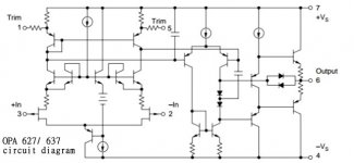
OPA627, LF351 circuit diagram reference
http://www.diyaudio.com/forums/attachment.php?attachmentid=620530&stc=1&d=1497108051
http://www.diyaudio.com/forums/attachment.php?attachmentid=620531&stc=1&d=1497108051
Subject title provides a reference in comparing the different between this cascode, two stages discrete pre-amp circuit.
http://www.diyaudio.com/forums/attachment.php?attachmentid=620530&stc=1&d=1497108051
http://www.diyaudio.com/forums/attachment.php?attachmentid=620531&stc=1&d=1497108051
Subject title provides a reference in comparing the different between this cascode, two stages discrete pre-amp circuit.
Attachments

Hi I came across this thread
I am looking at implementing a simple cascode pre amp between my DAC and power amp. The DAC ouputs 2V max, and I'd like a clean 4V signal, both incoming channels are balanced. Do you think this would work well for what I am intending?
**However I don't need or want volume attenuation in the circuit.
The DAC ouputs 2V max, and I'd like a clean 4V signal, both incoming channels are balanced.
The circuit's gain is around 21dB, but you lose 6dB since it's single ended.
So the net gain is 15dB, or around 9dB more than you want.
If R7 could be reduced to 30k, the circuit would have 12dB gain,
and (less the 6dB for being unbalanced) would have a net 6dB, as you want.
Last edited:
Rayma,
could this circuit be modified to be completely balanced from input to output?
I'm guessing I'd have to virtually double the components?
I have a little experience with upgrading components within an amplifier and some pretty serious crossover building, and I learned a little electronics with my degree (Automation), however I am certainly no electronics engineer.
- Status
- Not open for further replies.
- Home
- Source & Line
- Analog Line Level
- A cascode, two stage constant current discrete pre-amp circuit diagram