Good afternoon,
Last year I designed and built a 3-way active crossover network, using circuits pulled directly from the Linkwitz Lab site. The crossover was intended to replace a MiniDSP 2x4 and add outputs for subwoofers. It went together just fine and sounded pretty good, albeit a little warm. Fast forward to a few weeks ago, I was playing with a newly acquired Umik-1 and noticed that there was a definite high-frequency rolloff which is dependent on the position of the potentiometer used for volume control. Below are two traces, one with the pot at 50%, and one at 100%, with the source output level adjusted to give the same volume on the low end. Note that these were taken in my living room on a makeshift mic stand, so they aren't particularly pretty, but they do get the point across.

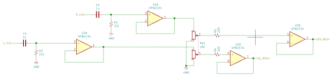
My first instinct was that this was due to the lack of a buffer between the volume pot and the high pass filter for the tweeter, as shown below. However, the rolloff seems to start well below the crossover point (1,250 Hz), with the levels already down ~2 dB at 700 Hz.


Above: Input HPF / buffer and volume pot (left), high pass which takes signal directly from the volume pot (right)
My attempt to solve this would be to add an additional buffer between the volume control and the filter stages, so there is no interaction between the pot and the other passive components involved. Can anyone guess as to whether this might solve the issue?
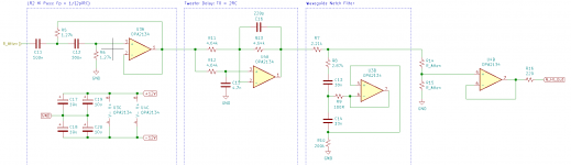
Additionally, if I am going to layout the board again, I wanted some input on the ordering of the filter stages. Linkwitz hints that the order is important on his page, but doesn't offer any advice as to the optimal layout. Here is the how they are currently arranged:

My main question is regarding the shelving low pass for the woofer baffle step compensation, since it is the only stage with a non-unity gain; should it be at the beginning of the woofer filter chain, as shown above, or at the end?
Finally, I wanted some general advice with the PCB layout. I'm not currently experiencing any issues with RF or weird noises, but I'm sure my layout could be improved. The only considerations I had in mind with the design were to put a small filter cap on the V+/V- pins of the opamps, and to try to keep power traces away from signal traces when possible. Here is the layout of the board I went with:


Are there any blatant issues that stick out in the above layout?
As always, thank you for reading and I appreciate any input that y'all might have.
Kellis
Last year I designed and built a 3-way active crossover network, using circuits pulled directly from the Linkwitz Lab site. The crossover was intended to replace a MiniDSP 2x4 and add outputs for subwoofers. It went together just fine and sounded pretty good, albeit a little warm. Fast forward to a few weeks ago, I was playing with a newly acquired Umik-1 and noticed that there was a definite high-frequency rolloff which is dependent on the position of the potentiometer used for volume control. Below are two traces, one with the pot at 50%, and one at 100%, with the source output level adjusted to give the same volume on the low end. Note that these were taken in my living room on a makeshift mic stand, so they aren't particularly pretty, but they do get the point across.
My first instinct was that this was due to the lack of a buffer between the volume pot and the high pass filter for the tweeter, as shown below. However, the rolloff seems to start well below the crossover point (1,250 Hz), with the levels already down ~2 dB at 700 Hz.
Above: Input HPF / buffer and volume pot (left), high pass which takes signal directly from the volume pot (right)
My attempt to solve this would be to add an additional buffer between the volume control and the filter stages, so there is no interaction between the pot and the other passive components involved. Can anyone guess as to whether this might solve the issue?
Additionally, if I am going to layout the board again, I wanted some input on the ordering of the filter stages. Linkwitz hints that the order is important on his page, but doesn't offer any advice as to the optimal layout. Here is the how they are currently arranged:
My main question is regarding the shelving low pass for the woofer baffle step compensation, since it is the only stage with a non-unity gain; should it be at the beginning of the woofer filter chain, as shown above, or at the end?
Finally, I wanted some general advice with the PCB layout. I'm not currently experiencing any issues with RF or weird noises, but I'm sure my layout could be improved. The only considerations I had in mind with the design were to put a small filter cap on the V+/V- pins of the opamps, and to try to keep power traces away from signal traces when possible. Here is the layout of the board I went with:
Are there any blatant issues that stick out in the above layout?
As always, thank you for reading and I appreciate any input that y'all might have.
Kellis
I like to say "draw the WHOLE circuit!" In this case, "all on one sheet!" You have a key point lost in the crack.instinct was that this was due to the lack of a buffer
Now we see a 1.27k filter, looking into up to 5k drive impedance. Of course it will shift the filter frequency down, and screw-up the alignment.
Filter theory specifies a source impedance. In active filters, this is often assumed to be Zero. For general audio filtering 10x or 100x smaller than the filter resistors.
Transpose the filter to 127k and 1nFd, drop the pot to 200 Ohms
 , or stick a buffer in there (or move pot to in front of U1A?). At 100:1 difference the error will be "small", but measurable on a sharp meter.
i would put decouping right at the power entry point on the pcb.
"shelving low pass for the woofer baffle step compensation" is in the mid branch? should be 1st?
see here regarding general topolgy:- https://www.diyaudio.com/community/...ssovers-a-la-linkwitz-multi-cascading.332562/ (my post at #10)
gain blocks if you have "hiss"
easier to set o/p level with pots, then replace with fixed r's
only one delay section?
o/p buffers?
Many thanks for the replies so far. It seems like the pragmatic approach will be to keep the pot where it is, but add a buffer after.
What size decoupling caps would you use? Big 1,000uF, or small ~10uF like on the op amp pins?
Yes, the shelving low pass is on the woofer / mid branch. I am using woofer and mid interchangeably since it's a 2 way + sub system, the woofer is the middle driver - perhaps that's confusing.
There are attenuation resistors on the outputs, I've just been leaving lots of lead attached when I solder them to the board so they're easy to change out. I've been trying to keep their values low (~1kR) to keep the output impedance low ish and avoid adding an output buffer. Would it be smart to add one anyway?
i would put decouping right at the power entry point on the pcb.
"shelving low pass for the woofer baffle step compensation" is in the mid branch? should be 1st?
see here regarding general topolgy:- https://www.diyaudio.com/community/...ssovers-a-la-linkwitz-multi-cascading.332562/ (my post at #10)
gain blocks if you have "hiss"
easier to set o/p level with pots, then replace with fixed r's
only one delay section?
o/p buffers?
What size decoupling caps would you use? Big 1,000uF, or small ~10uF like on the op amp pins?
Yes, the shelving low pass is on the woofer / mid branch. I am using woofer and mid interchangeably since it's a 2 way + sub system, the woofer is the middle driver - perhaps that's confusing.
There are attenuation resistors on the outputs, I've just been leaving lots of lead attached when I solder them to the board so they're easy to change out. I've been trying to keep their values low (~1kR) to keep the output impedance low ish and avoid adding an output buffer. Would it be smart to add one anyway?
Ok thanks for the help so far. Looking back over my schematic, I have 4x unused opamp halves, so it seems silly not to add output buffers. I can think of two ways to go about this: putting the attenuation resistors before a unity gain line driver, or setting the gain to be <1 using a voltage divider on the inverting terminal. Is either of these methods preferable over the other? Here's how that would look on the tweeter filter chain, for example:

Option A: attentuation resistors before line driver

Option B: using resistors to set opamp gain <1
Option A: attentuation resistors before line driver
Option B: using resistors to set opamp gain <1
Your Sallen/Key filter still needs a buffer on its input because it came from the passive attenuator.
Your allpass tweeter delay filter needs a buffer on its input since the waveguide notch (which is a
gyrator) has varying output impedance with frequency.
Your option B output stage has gain > 1, you have to use an inverting opamp stage for gain less than 1 (well
strictly between 0 and -1 to be precise). Non-inverting topology is always > 1 gain unless its a follower and
then its exactly 1.
Basically any filter stage that's not being driven from the output of the previous opamp needs a buffer on its
input to provide zero source impedance - all these opamp filter circuits assume this.
Your Sallen/Key filter still needs a buffer on its input because it came from the passive attenuator.
Your allpass tweeter delay filter needs a buffer on its input since the waveguide notch (which is a
gyrator) has varying output impedance with frequency.
I think this can be accomodated by sandwiching the volume pot between two buffers, and then rearranging the tweeter filters so that the notch filter comes after the delay - this way, the notch input is tied directly to the output of the delay opamp (see attached).
I am not sure if the attenuation resistors are OK where they are at, or if they need to be after the output buffer so they don't affect the notch filter. Thank y'all for the advice so far!
Attachments
- Home
- Source & Line
- Analog Line Level
- Active Crossover Volume Control, Stage Ordering, & Board Layout