This post is related to a build I've been mostly discussing (learning from) with @abraxalito, but it goes into a more general question that pushed me to create a new thread about it. Obviously not a new topic either, but it's really puzzling me.
As part of a project, I'm bringing together an ADC chip (AK5381) and a stack of multibit DACs (TDA1387) via an Arduino M4 I2S ports (Teensy4). All powered on batteries with independent voltage regulators or current sinks. Problem is, on the breadboard I occasionally got unbearable avalanches of noise out of the DAC. At first it would run ok, but after a few seconds the avalanche of cracking noise would start and continue until turned off. The noise was related to the DAC, without it the ADC would give clean readings on the MCU. I experience the same problem with another DAC (AK4384). I tried different voltage regulators and nothing really worked. Pretty much discarded everything I could and I'm very suspicious of a ground problem, or lack of proper ground.
The overall circuit is pretty complex but I'm putting it into a PCB in Eagle and got to the point of creating ground planes for all three sections: analog, digital and shared. The Mickey Mouse model in my mind, without much experience and research about the subject.
The ADC has independent analog and digital pins, but the DAC doesn't. Should the DAC ideally be located and grounded around the shared area, where the ADC's AGND and DGND meet? Are there any guidelines or important techniques to consider, such as use of ferrites or inductors, other than decoupling capacitors at power supplies? These are things I'm wondering about, mostly hunted by the ghost of manufacturing board prototypes that will welcome me with furious noise accompanied by the question "why didn't you ask before".
As frequencies go up, one continuous ground plane for everything is recommended. At lower RF frequencies such as for (perhaps non-oversampling) dacs, split ground planes are still sometimes used.
Some reading material might include:
https://www.analog.com/media/en/training-seminars/design-handbooks/Basic-Linear-Design/Chapter12.pdf
https://www.maximintegrated.com/en/design/technical-documents/app-notes/3/3491.html
Also it might help if we could see a schematic for what you are trying to build.
May I ask if you have a scope and or other test equipment?
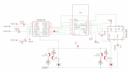
Hi Mark, thanks for your interest! I prepared a few pictures on what I'm dealing with, selected to bring it to the point.
On the right is the DAC, on the left the ADC. In the middle the ARM M4 MCU. Power supply of the MCU is a single Li-Ion battery (3.3V regulated). The supply of the DAC and ADC is a stack of batteries 'regulated' by a pair of current sinks, visible in the lower part of the schematic. Grounds are currently wired without planes in the diagram.
My question is mostly where should the parts be ideally located and how the plane(s) should look like. The DAC has only one ground pin, as mentioned before, where I2S digital data will meet the AC analog signal. Digital data will flow to the MCU back and forth, so I try to bring it as close as possible to it. But power supply current and analog audio will flow instead to the current source. Same with the ADC. I can't quite visualise how can be both things combined on a single plane.
Thanks for the readings. They might lead me to an answer, any hints are appreciated.
I don't have more than a decent multimeter here. I'm moving a lot. But once the board is printed I'll have access to a scope (and someone who knows how to use it) to test it.
On the right is the DAC, on the left the ADC. In the middle the ARM M4 MCU. Power supply of the MCU is a single Li-Ion battery (3.3V regulated). The supply of the DAC and ADC is a stack of batteries 'regulated' by a pair of current sinks, visible in the lower part of the schematic. Grounds are currently wired without planes in the diagram.
My question is mostly where should the parts be ideally located and how the plane(s) should look like. The DAC has only one ground pin, as mentioned before, where I2S digital data will meet the AC analog signal. Digital data will flow to the MCU back and forth, so I try to bring it as close as possible to it. But power supply current and analog audio will flow instead to the current source. Same with the ADC. I can't quite visualise how can be both things combined on a single plane.
Thanks for the readings. They might lead me to an answer, any hints are appreciated.
May I ask if you have a scope and or other test equipment?
I don't have more than a decent multimeter here. I'm moving a lot. But once the board is printed I'll have access to a scope (and someone who knows how to use it) to test it.
Attachments

Looks like you may have some problems.
Maybe useful to read about series termination of transmission lines, if you haven't done so already. Applies to clock and I2S bus signals:
https://www.ctscorp.com/wp-content/uploads/2015/10/AN1025.pdf
For dacs sometimes over-damping (or a certain type of mismatched-termination) can sometimes sound better. In that case the source series termination resistor might be more like 100R instead of closer to 33R.
Also, you might be better off with the ARM a bit physically further away from the data converters. Data converters are mixed-signal devices that have a very significant analog part of them. OTOH, MCUs tend to generate a lot of switching/clock noise which can be bad for the analog sections of data converters.
Regarding a scope, you need one for this type of work. And IMHO you must learn how to use it including detailed knowledge of using the probes. Tek has some good app notes on the subject I could link to if you are interested enough to study up on it. A fair amount to learn, but, again IMHO, essential for what you are doing.
Last edited:
I am thinking of making an audio to I2S adaptor for testing my dacs but can't find the AKM5318. (avoids the need to use a test CD)
There is an AKM 5538 which is 8 channels - is this the one?
There is an AKM 5538 which is 8 channels - is this the one?
Yes @batteryman I meant the AK5381. There's a typo mistake in the diagram sorry for that. I found some of these chips online, old stock, and desoldered it also from an old obsolete Tascam USB interface, which I got for almost no price. It sounds very neutral and precise subjectively, compared to more swampy but harmonic PCM1802 which I tried before.

Looks like you may have some problems.
Maybe useful to read about series termination of transmission lines, if you haven't done so already. Applies to clock and I2S bus signals:
https://www.ctscorp.com/wp-content/uploads/2015/10/AN1025.pdf
For dacs sometimes over-damping (or a certain type of mismatched-termination) can sometimes sound better. In that case the source series termination resistor might be more like 100R instead of closer to 33R.
Also, you might be better off with the ARM a bit physically further away from the data converters. Data converters are mixed-signal devices that have a very significant analog part of them. OTOH, MCUs tend to generate a lot of switching/clock noise which can be bad for the analog sections of data converters.
Regarding a scope, you need one for this type of work. And IMHO you must learn how to use it including detailed knowledge of using the probes. Tek has some good app notes on the subject I could link to if you are interested enough to study up on it. A fair amount to learn, but, again IMHO, essential for what you are doing.
Thanks again @Markw4 for the documents shared. I read them carefully, followed by a number of related articles I found.
http://www.hit.bme.hu/~papay/edu/Acrobat/GndADCs.pdf
https://d1.amobbs.com/bbs_upload782111/files_11/ourdev_445151.pdf
https://www.ti.com/lit/an/slyt512/slyt512.pdf
They are clear on that DGND and AGND must be generally tied together under the converter(s), on a single plane and paying much attention on that digital and analog return currents don't cross their ways. This is usually done with split planes bridged close to the converter, or simply 'partitioned' on different zones of a flat plane. The last seems more suited to me, since I'm working with 2 converters an ADC and a DAC. Important I read is that return currents naturally travel as close as possible to their positive tracks, also for instance that the decoupling caps of each AGND and DGND pins must be fast ceramics and grounded to their respective 'ground zones'.
In my system there is an aluminium chassis where the grounds of both independent power supplies (digital and analog) meet. Say the chassis is my star ground point. Most articles repeat that digital and analog grounds meet at the power supplies, so I seem to alright there. But I've also often read that both grounds should only meet where the converters are located, I assume to avoid a ground loop between both 'meeting points'.
I'm puzzled. Is it a good practice to join the power supplies negative poles at the chassis? Or should they only meet at the ground plane where the converters are located, preferably where the converter chips are?
Hope this question makes any sense and has an easy answer. Please consider it open to anyone who has word on it.
PD: @Markw4, if you could point me to an intro document on oscilloscopes and any affordable to start with, preferably digital if taking up less physical space... I will appreciate it very much.
Oscilloscope info:
https://download.tek.com/document/ABCs of Probes 60W-6053-15.pdf
https://download.tek.com/document/03W_8605_7_HR_Letter.pdf
Regarding power ground planes, many people now recommend to use only one ground plane for both analog and digital. In some special cases it may make sense to use keepouts and or slots, but one has to be very careful not to inadvertently make an antenna that way. Also, I don't know of any reason why using a single ground plane can't be made to work. If there are to be two ground planes then you might want to stack them, one ground plane per layer. There would be some EM coupling between them, but there is some isolation too.
Regarding power supply grounding, especially if they are external from the ADC/DAC PCB, I only ground them at the load (in this case the ADC/DAC PCB). Otherwise ground loops are formed. Also, for external power supplies if they are, say, for example, +-15v, then I run a separate ground for +15 and for -15v. The grounds only get connected together at the load. Also, sometimes I use the same positive regulator type for both +15v and for -15v. One of them just gets used 'upside down' to produce the -15v rail (the + end of that regulator is tied to ground at the load). That way both +-15v rails have the exact same frequency response, and the same output impedance verses frequency. Some people say SQ is better if both rails have matched performance. To do that each 15v supply needs to have its own dedicated transformer winding. Center-tapped transformer windings won't work for that if the center-tap connection has to be shared by the two regulators.
A good write up on ground planes:
https://www.analog.com/en/analog-dialogue/articles/staying-well-grounded.html
Hal
https://www.analog.com/en/analog-dialogue/articles/staying-well-grounded.html
Hal
Also one (two) from TI, but I think the AD one is better IMO
https://www.ti.com/lit/an/slyt499/slyt499.pdf
https://www.ti.com/lit/an/slyt512/slyt512.pdf
Hal
https://www.ti.com/lit/an/slyt499/slyt499.pdf
https://www.ti.com/lit/an/slyt512/slyt512.pdf
Hal
Try using digital isolators, put the Teensy4 on separate ground plane(s) and the isolator over the split of the planes.
Like with this codec (it uses Teensy3.6 though):
https://github.com/whollender/SuperAudioBoard
https://github.com/whollender/SuperAudioBoard/blob/master/SuperAudioBoardDesignGuide.pdf
I think the measurements were made and were excellent. Only drawback these days is the availability of the isolator chips.
I have a little situation here. What to do with return currents when a cut on the ground plane MUST be?
The plane on the left and right are at different voltage, because of a ground lift on which an invisible DAC at the left is working. The board is only two layers and a line (AOUT) must land from the ground on the left to the other. Say... to get decoupled from lifted DGND to base GND.
It occurred to me shielding the line on the sides, surrounding the line all the way with the source ground. I tried to illustrate it pictures below. Is this a good idea or even a practice?
Attachments


Can you show the different grounds schematically? How much of the PCB surface area are the different ground areas? Are the grounds connected anywhere? If so, where? What is the maximum clock frequency the dac will run at? How fast do you need clock risetime to be?
Can you show the different grounds schematically? How much of the PCB surface area are the different ground areas? Are the grounds connected anywhere? If so, where? What is the maximum clock frequency the dac will run at? How fast do you need clock risetime to be?
Schematically is a bit difficult and messy, but here is a broad view of the planes. I seem to have sorted it out setting the planes on the different layers: DGND Blue (+3V), AGND Red (0V). This allows me to "hook up" grounds into each other as tracks transit the gap. DGND connects to GND on the point marked by a yellow circle, through a BJT PNP actually.
MCU is Teensy 4 running at 150MHz. DAC is an AK4384 not sure what maximum clock would be but here is a datasheet.
Attachments


Okay. It looks like AK4384 might run on an MCLK up around 25MHz. Depending on MCLK rise and fall times, clock signal bandwidth can be calculated as described at: https://www.edn.com/rule-of-thumb-1-bandwidth-of-a-signal-from-its-rise-time/
For an audio clock example, say we take Crystek 957. Rise time is specified as: 3ns Max @ 20% to 80% Vcc. Probably in most cases rise time will be faster. Maybe closer to something like, say, for example, 1.5ns.
You can probably figure out from the above link that you have some pretty high frequency components in those clock edges. The problem seen a lot today with split analog and digital ground planes is the ground planes slots (gaps or cuts) can form a resonant antenna structure out of the ground plane. Didn't used to be a problem so much way back when audio dacs were clocked at only a handful of MHz and rise times were not so fast.
Part of the question here would if this board is for some commercial purpose? If it is then it has to comply with government rules for EMI/RFI emissions. If its acting like an antenna, that's bad. OTOH, if its for personal use probably nobody is going to complain you are causing interference with their electronic equipment.
Anyway, with higher clock speeds and faster rise times its usually best these days to use a continuous unslotted/un-cut ground plane. It is possible to stack continuous ground planes if you have enough layers, and you want to do that. There would be some coupling between them, but that might be okay. Or, its possible to use only one single ground plane shared by both analog and digital. In cases like that you may have to think more carefully about layout so that high frequency digital ground currents tend not flow too much in the ground plane area where your analog circuitry is located.
In fact the videos a few posts up give some useful advice that you might find helpful. Maybe you already watched them but you still have concerns?
Also, when you say a cut in the ground plane 'must be,' its not clear that it really must be or maybe its more like you tend to worry not having a cut could potentially hurt SQ?
Okay. It looks like AK4384 might run on an MCLK up around 25MHz. Depending on MCLK rise and fall times, clock signal bandwidth can be calculated as described at: https://www.edn.com/rule-of-thumb-1-bandwidth-of-a-signal-from-its-rise-time/
For an audio clock example, say we take Crystek 957. Rise time is specified as: 3ns Max @ 20% to 80% Vcc. Probably in most cases rise time will be faster. Maybe closer to something like, say, for example, 1.5ns.
You can probably figure out from the above link that you have some pretty high frequency components in those clock edges. The problem seen a lot today with split analog and digital ground planes is the ground planes slots (gaps or cuts) can form a resonant antenna structure out of the ground plane. Didn't used to be a problem so much way back when audio dacs were clocked at only a handful of MHz and rise times were not so fast.
Part of the question here would if this board is for some commercial purpose? If it is then it has to comply with government rules for EMI/RFI emissions. If its acting like an antenna, that's bad. OTOH, if its for personal use probably nobody is going to complain you are causing interference with their electronic equipment.
Anyway, with higher clock speeds and faster rise times its usually best these days to use a continuous unslotted/un-cut ground plane. It is possible to stack continuous ground planes if you have enough layers, and you want to do that. There would be some coupling between them, but that might be okay. Or, its possible to use only one single ground plane shared by both analog and digital. In cases like that you may have to think more carefully about layout so that high frequency digital ground currents tend not flow too much in the ground plane area where your analog circuitry is located.
In fact the videos a few posts up give some useful advice that you might find helpful. Maybe you already watched them but you still have concerns?
Also, when you say a cut in the ground plane 'must be,' its not clear that it really must be or maybe its more like you tend to worry not having a cut could potentially hurt SQ?
Thank you Mark for all the information. A lot to research and indeed the planes acting like an antena is one of my concerns. The board might be used by myself or others close to other audio equipment, even though in an aluminium case it should act as an EMI source ideally. But maybe I wasn’t clear enough with the “must be” separated grounds. In the circuit I’m designing DAC, ADC and MCU are grounded at a higher voltage than AGND (4-3V higher). This is to simplify the output stage of the DAC/>amplifier among other reasons. Would I use a single plane for both there would be a short and smoke.
I’ve tried to place everything correctly as close as possible to their ground points (digital has its own power source with ground on the blue zone) and lines crossing the gap are the strictly necessary. Will the planes interact and be an EMI source even if there there are no return currents badly routed?
- Home
- Source & Line
- Digital Line Level
- ADC + DAC (I2S) ground planes PCB