Here is my take on the balanced input LM3886 implementation.
Edited on 6-5-2022 with many small improvements to the schematics.
Edited on 7-16-22.
Edited on 12-23-2022
The gain for the LM3886 was eventually set to 10.
Circuit topology is an instrumentation amplifier. Balanced signal is fed into high-pass filter (100R, 100pF). We then have LM4562 opamp to provide impedance matching to the inputs of the LM3886. LM3886 chip amp is then fed two differential signals to its inverting and noninverting inputs and acts as a difference amplifier.
The gain of the LM3886 is set to 10 and is defined by the relation of the feedback resistor Rf = 20K and the input resistor Ri = 2K. Because we are using the chip amp at its minimum stable gain of 10, the stability network of Cf and Rfs is modified to omit the resistor. Otherwise, the gain of the amp is divided in two at the frequency of Cf and would equal to 5 - potentially a source of instability (in my opinion).
To ensure the HF stability two 27pF capacitors are added.
Resistors R8, R9, R10, and R11 determine CMRR or the whole circuit and should be at least 0.1% tolerance - this will allow for theoretical 66 dB CMRR. Better tolerances will allow for better CMRR, but will be limited by CMRR rating of the LM3886 itself.

Just a side note: 10K resistor has Johnson noise that is -112 dBU (across 20KHz range, at 20 degrees C) - according to this online calculator: https://www.daycounter.com/Calculators/Thermal-Noise-Calculator.phtml.
Feedback resistor Rf and input resistor Ri are both connected to the inverted input of the chip amp. To balance that, we need to mirror the same values for non-inverted input, except we connect resistors to the input and to the ground. This arrangement created what is known as a difference amplifier.
Since both input resistors are 2K we need a buffer to interface to the outside world and to be able to present at least 10K of impedance to connected devices.
Differential input resistance is 2 * 47K = 94K.
Common mode resistance is 47K + 2 * 2.2M = 4.447Meg.
For the balanced inputs the level of the signal is usually 4Vrms per channel. Half of that is 2. After RMS conversion 2 * √2 = 2.8284 Vpk. With the minimum gain of 10, the output voltage chip amp has to be able to handle is therefore 2.8284 Vpk * 10 = 28.284 Vpk. This is possible because LM3886 can be powered +-28V max into 4 ohm loads.
Dissipated power is another factor that determines maximum allowable power output by the LM3886:
Pd = Vcc^2 / 2* Pi^2 *Rload
For 28V supply and 4 ohms load: Pd = 784 / 19.7292 = 39.7380W
For 30V supply and 4 ohms load: Pd = 900 / 19.7292 = 45.6407W
Note that non insulated LM3886 can dissipate 40W without the fan, and insulated LM3886 can only dissipate 30W.
In our case, power supply is +-28V. We also need to subtract up to 5V for 4 ohm loads and 2.7V for 8 ohm due to chip voltage drop. 28V - 5V = 23Vpk of max output voltage swing without the distortion.
In the schematics input buffers are configured with the gain of 1+ 2 * 1K / 20K = 1 + 0.1 = 1.1. The gain of the differential stage is 10. Total gain is 10 * 1.1 = 11.
Edited on 6-5-2022 with many small improvements to the schematics.
Edited on 7-16-22.
Edited on 12-23-2022
The gain for the LM3886 was eventually set to 10.
Circuit topology is an instrumentation amplifier. Balanced signal is fed into high-pass filter (100R, 100pF). We then have LM4562 opamp to provide impedance matching to the inputs of the LM3886. LM3886 chip amp is then fed two differential signals to its inverting and noninverting inputs and acts as a difference amplifier.
The gain of the LM3886 is set to 10 and is defined by the relation of the feedback resistor Rf = 20K and the input resistor Ri = 2K. Because we are using the chip amp at its minimum stable gain of 10, the stability network of Cf and Rfs is modified to omit the resistor. Otherwise, the gain of the amp is divided in two at the frequency of Cf and would equal to 5 - potentially a source of instability (in my opinion).
To ensure the HF stability two 27pF capacitors are added.
Resistors R8, R9, R10, and R11 determine CMRR or the whole circuit and should be at least 0.1% tolerance - this will allow for theoretical 66 dB CMRR. Better tolerances will allow for better CMRR, but will be limited by CMRR rating of the LM3886 itself.
Just a side note: 10K resistor has Johnson noise that is -112 dBU (across 20KHz range, at 20 degrees C) - according to this online calculator: https://www.daycounter.com/Calculators/Thermal-Noise-Calculator.phtml.
Feedback resistor Rf and input resistor Ri are both connected to the inverted input of the chip amp. To balance that, we need to mirror the same values for non-inverted input, except we connect resistors to the input and to the ground. This arrangement created what is known as a difference amplifier.
Since both input resistors are 2K we need a buffer to interface to the outside world and to be able to present at least 10K of impedance to connected devices.
Differential input resistance is 2 * 47K = 94K.
Common mode resistance is 47K + 2 * 2.2M = 4.447Meg.
For the balanced inputs the level of the signal is usually 4Vrms per channel. Half of that is 2. After RMS conversion 2 * √2 = 2.8284 Vpk. With the minimum gain of 10, the output voltage chip amp has to be able to handle is therefore 2.8284 Vpk * 10 = 28.284 Vpk. This is possible because LM3886 can be powered +-28V max into 4 ohm loads.
Dissipated power is another factor that determines maximum allowable power output by the LM3886:
Pd = Vcc^2 / 2* Pi^2 *Rload
For 28V supply and 4 ohms load: Pd = 784 / 19.7292 = 39.7380W
For 30V supply and 4 ohms load: Pd = 900 / 19.7292 = 45.6407W
Note that non insulated LM3886 can dissipate 40W without the fan, and insulated LM3886 can only dissipate 30W.
In our case, power supply is +-28V. We also need to subtract up to 5V for 4 ohm loads and 2.7V for 8 ohm due to chip voltage drop. 28V - 5V = 23Vpk of max output voltage swing without the distortion.
In the schematics input buffers are configured with the gain of 1+ 2 * 1K / 20K = 1 + 0.1 = 1.1. The gain of the differential stage is 10. Total gain is 10 * 1.1 = 11.
Attachments


Last edited:


Got PCBs in the mail and the process has started!
Will need to make a few adjustments for the PCB:
1. Mute capacitor increased to 100uF - footprint increased accordingly
2. 470uF capacitors can be electrolytic with positive facing towards the LM3886 inputs
Will need to make a few adjustments for the PCB:
1. Mute capacitor increased to 100uF - footprint increased accordingly
2. 470uF capacitors can be electrolytic with positive facing towards the LM3886 inputs
Attachments

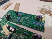


More parts were soldered in:
Attachments


Just 2 remarks :
1) LM3886 is stable with 10k/100k resistors at the feedback network.
2) If I need a net differential gain of 3 with symmetrical inputs, this is what I would do.
It is not LM3886, but it illustrates the principle.
View attachment 1059397
Cheers,
Patrick
As long as the gain is more then 10 , LM3886 is stable. 100k/10k gives gain of 10. 10k/1k gives gain of 10 too.
Having Lm4562 as buffers allows to preserve CMRR of difference amp. You can read more in THAT12xx datasheet, pages 4 and 5 - https://www.mouser.com/datasheet/2/407/THAT_1200-Series_Datasheet-532288.pdf
I have discussion on similar topic here - https://www.diyaudio.com/community/...-is-better-to-choose-as-a-summing-amp.386600/
Last edited:
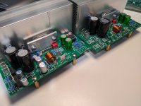
Heatsinks are mounted!
Had to clean flux from the boards before doing that. 70% isopropyl alcohol and the toothbrush helped a lot lol. Took about 15min for each of the boards.
Had to clean flux from the boards before doing that. 70% isopropyl alcohol and the toothbrush helped a lot lol. Took about 15min for each of the boards.
Attachments


Last edited:
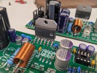
Photo dump of assembled PCBs.
Attachments
-
 PXL_20220630_004851285.jpg370.9 KB · Views: 131
 -
 PXL_20220630_004848933.jpg378.1 KB · Views: 115
 -
 PXL_20220630_004856399.jpg452 KB · Views: 123
 -
 PXL_20220630_004829293.jpg424 KB · Views: 127
 -
 PXL_20220630_004838003.jpg411.2 KB · Views: 127
 -
 PXL_20220630_004835866.jpg355.1 KB · Views: 133
 -
 PXL_20220630_004821223.jpg366.3 KB · Views: 142
Fully assembled photos
Attachments
-
 PXL_20220703_010526633.jpg301.9 KB · Views: 146
 -
 PXL_20220703_010519455.jpg310.6 KB · Views: 141
 -
 PXL_20220703_010505611.jpg222.3 KB · Views: 144
 -
 PXL_20220703_005608417.jpg396.8 KB · Views: 159
 -
 PXL_20220703_005612032.jpg418.8 KB · Views: 160
 -
 PXL_20220703_005616050.jpg444.2 KB · Views: 152
 -
 PXL_20220703_005628250.jpg319.9 KB · Views: 152
If you know ahead of time that you'll be cleaning the boards, I highly recommend using solder with water soluble flux. Alternatively RMA flux with some actual flux cleaner works well. I write quite a bit on that here: https://neurochrome.com/pages/choosing-solderHad to clean flux from the boards before doing that. 70% isopropyl alcohol and the toothbrush helped a lot lol. Took about 15min for each of the boards.
How does your amp behave as it enters/exits clipping with a 4 Ω load?
Tom
I am quite interested to measure the performance myself. It will take some time though - I need to do research on tools.
So far the plan is to use my Focusrite Scarlett audio interface for measurements. I also bought two 8ohm 100w resisors to measure both 4ohms and 8 ohms loads.
I also have Crown xls1000 amp that I want to measure too. It's class D and I suspect it has some weird thing going on with the frequency response.
Two LM3886 that were used in this amp were repurposed from the first build - non-inverted schematics straight from datasheet implementation (with stability components). The reason that it did not satisfy was those ground loops from the USB hub built in my monitor. USB hub was used to power Focusrite Scarlett audio interface. Unbalanced signal was then taken into the non-inverted amp.
No, but might need to invest into one...Do you have an oscilloscope?
Tom
Maybe this one ($27) - Treedix DSO138 Oscilloscope DIY Kit Handheld Digital Oscilloscope 1msps Real-Time Sampling Rate 2.4 inch TFT Display https://a.co/d/3zlJJe0
Or this one ($197) - Hantek DSO2C10 2 CH Oscilloscope Without Built-in DDS Generator, 100MHz 1GSa/s https://a.co/d/0DjmJbq
Was listening the amplifier today and was surprised how much power single LM3886 can produce. It can do very loud! Sounds clean with no distortion that I can catch with my ears. Will try measuring THD in the future. Heatsinks got pretty hot to the touch, but seem to be able to dissipate the heat just fine.
Today swapped LM4562 chips for NE5532 - no difference that I can hear with my ears.
After leaving the amp on for a few days without input signal, two heatsinks were pretty warm to touch. I'm thinking it could be because the amp oscillating without signal in?
After leaving the amp on for a few days without input signal, two heatsinks were pretty warm to touch. I'm thinking it could be because the amp oscillating without signal in?
- Home
- Amplifiers
- Chip Amps
- Balanced input LM3886 design and PCB layout