Hi folks
I want to build an output stage for current output DACs such as the PCM61 so I have been looking at I-V conversion methods.
Rather than use the op-amp built into the PCM61 it is better to use an external opamp with better specs. The op-amp inside the PCM61 DAC chip has a slew rate of only 12V/uSec but to properly reproduce the signal coming out of the DAC the opamp should have a slew rate of 1000V/uSec.
The AD811 has been widely used for I-V conversion and has a slew rate of 2500V/uSec. I don't have any of those and they are expensive, but I do have several AD812s, which is the dual version and has a slew rate of 1600V/uSec.
The PCM61 also requires the external opamp to have close to zero input impedance, which the AD811 offers.
Anyways, after research I found lots of people had successfully used the AD811 with the PCM61 or one of the similar Burr-Brown DACs.
I don't see any reason why I can't substitute the AD812, but I haven't been able to find any circuit schematics specifically for the AD811/2 as an I-V converter.
So does anyone have a suitable schematic for an I-V converter using the AD811/2, or can I just use something like the scheme present by Herbert Rutgers:
https://www.by-rutgers.nl/IV-converter.html
Slew rate is only part of why AD811 is eminently suitable as an I-V converter in conjunction with the PCM61.
AD811 can provide a dynamic impedance of less than 1 ohm, it also works well at unity gain and as a buffer.
But bottom line, AD811 works very well in the application I am interested in and having looked at the specs, I see no reason why the dual version AD812 shouldn't also work well, and as I already have the AD812s...
AD811 will provide close to 6V pp of output at a very low distortion levels, while keeping the voltage swing at Iout DAC pin well below the compliance threshold, allowing all Iout DACs to perform at their best as well.
The problem with 811 is in its correct implementation, which is quite hard due to its max Vcc/Vee limitation, huge bias, and very fast speed that requires careful layout and parts' selection to prevent oscillations and rise in THD.
Last edited:
Unfortunately your AD811 is a current feedback amp like most video amps.
With your circuit you build a 200MHz oscillator
With your circuit you build a 200MHz oscillator
Yes, AD811/2 is difficult to implement, hence I asked about specific schematics.
However, I have read in many places that it is worth the effort to tame the AD811.
However, I have read in many places that it is worth the effort to tame the AD811.
Much better solution is CFB OP's like very a fast AD811. The compliance voltage swing I have achieved is 2.5 mV max -> with 1 kHz square wave at 0dB (!!) - extremely harsh / demanding. The frequency response is flat from 16Hz to 22 kHz within 0.1 dB. AD811 has higher input offset voltage and input bias current, but that’s nothing (negligible) compared to ability to present itself to 1704 as flat, very low dynamic impedance load. It is like perfect resistor with constant resistance, with added capabilities of providing the gain that can be optimised by selecting Rf and Rg to suit preceding filters / oversamplers. For the first time I was able to listen to natural, uncoloured digital reproduction with no fatigue of any kind. The estimated dynamic impedance is around 1 ohm and is flat across the required frequency range. The topology is dual differential 1704 implementation in very low noise environment, with noise levels at all Vcc / Vee pins equal to ground plane noise levels. I did not have AD811 oscillations’ issue of any kind…
adequate power supply and decoupling are essential for faster OpAmps.
There are few areas that need attention with CFB amplifiers. Keeping them stable is not easy... I suppose some experience with RF designs could help. Apart from outstanding sound in I/V application, they are quite educational in a way that everything has to be almost perfect to get them perform adequately.... and that is a challenge. Latter, VFB amplifier can be dropped in if that is preferable; they will also benefit from optimised “surrounding environment”... but, once you try CFB you will not go back to VFB... and very son you will realise that various OP amplifier will not be considered any more as devices that will colour the sound, but as a silicon gain stages…
Last edited:
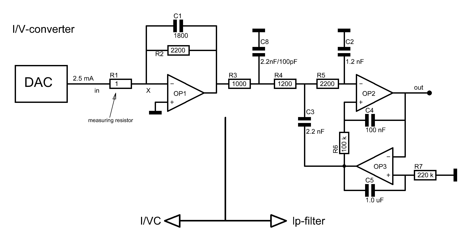
There is a schematic in an old Walt Jung article, but I'm not sure if it is usable in the form Jung presented:
Attachments


Last edited:
Spec-wise, AD812 is rather a long way from being a dual AD811. But its certainly usable as I/V. The main drawback I've found in using CFB in I/V applications is noise and AD812 is noisier than AD811.
You might find this article useful in designing filters using CFB opamps : https://www.ti.com/lit/an/slyt081/slyt081.pdf
You might find this article useful in designing filters using CFB opamps : https://www.ti.com/lit/an/slyt081/slyt081.pdf
Hi Abraxalito, cheers, I shall study that article iwth interest.
BTW, what solution do you happen to prefer for I-V conversion? I know you have been mostly working with the TDA1387 and I am using the PCM61, but wouldn't what works well with one also work well with the other?
BTW, what solution do you happen to prefer for I-V conversion? I know you have been mostly working with the TDA1387 and I am using the PCM61, but wouldn't what works well with one also work well with the other?
Currently (pun intended) my preferred solution is just a common-gate MOSFET. The DAC feeds the source terminal and an LC filter connects to the drain. Then I use an opamp after that, in inverting mode - its input resistor forms the terminating load for the filter.
I'm doubtful if that scheme can be made to work with PCM61 though as I suspect it does not have the output compliance flexibility that TDA1387 has. I will check the DS though to be sure.
I'm doubtful if that scheme can be made to work with PCM61 though as I suspect it does not have the output compliance flexibility that TDA1387 has. I will check the DS though to be sure.
right, so with the internal impedance of the dac (1.3k) the input sucks away a lot of current. Even with 65 ohm there will be only 1/20 current
The noise and distortion will be horrendous(<<-100dB) compared to modern opamps, even if you get the input right
The noise and distortion will be horrendous(<<-100dB) compared to modern opamps, even if you get the input right
With I/V circuits, I find it helpful to keep in mind that the high-speed transitions between samples is not part of the desired signal. Most of the wideband, high slew-rate handling active circuitry utilized in I/V circuit design is only there to handle the transistion between samples, without introducing value errors to the samples themselves. The trick to easing these demands on the I/V circuit, is to bandlimit the sample transistions before they are fed to any active circuit. Passive filtering can serve that purpose, but care must be taken to ensure that the I/V node is not, thereby, made resonant as a consequence.
right, so with the internal impedance of the dac (1.3k) the input sucks away a lot of current. Even with 65 ohm there will be only 1/20 current
But the input impedance is much, much lower than that in practice because the device is used with NFB. So in practice it will 'suck away almost all the current'. Which is what is wanted with an I/V.
The 65ohm and 14ohm input impedances are given open-loop.
With I/V circuits, I find it helpful to keep in mind that the high-speed transitions between samples is not part of the desired signal. Most of the wideband, high slew-rate handling active circuitry utilized in I/V circuit design is only there to handle the transistion between samples, without introducing value errors to the samples themselves. The trick to easing these demands on the I/V circuit, is to bandlimit the sample transistions before they are fed to any active circuit. Passive filtering can serve that purpose, but care must be taken to ensure that the I/V node is not, thereby, made resonant as a consequence.
I agree Ken - adding the passive filter prior to the I/V stage considerably eases the burden on the I/V opamp. But the issues go beyond ensuring the filter doesn't resonate, the primary issue with many DACs (including PCM61) is that of DAC output compliance. Introducing the filter may well mean the 'virtual earth' the DAC expects isn't sufficiently close to 'earth' any longer.
Given that PCM61 has been around a longtime and many people have designed & implemented successful output stages for it, I figured there was no sense in re-inventing the wheel, but other than valve/tube solutions, I haven't yet found any detailed schematics that I can work from - hence this thread. It seems that there are two primary methods that people have used - an opamp based i-v converter or a simpler i-v resistor followed by gain stage. I'm happy to try any solution as part of the learning process.
...Introducing the filter may well mean the 'virtual earth' the DAC expects isn't sufficiently close to 'earth' any longer.
Agreed, Richard.
Also, excuse my inadvertent double posting above.
Last edited:
There is a schematic in an old Walt Jung article, but I'm not sure if it is usable in the form Jung presented:
The AD811 can be used for i / v according to a schematic from old W. Jung article.
I used them a long time ago in two of my projects with TDA1541 and PCM1702 for the i / v stage. The supply voltage was +/- 8V from the W. Jung superregulator as seen from the pictures.
The sound was great especially with the PCM1702, however shortly after this I switched to the tubes for the i / v stage which I still use today.
But now I'm doing a new DAC with TDA1547 and I'm thinking of using the AD811 again.
With the AD811 you should pay attention to the PCB and not give it too high supply voltage because then you need to mount small heatsink on them, that's why I used +/- 8V.
Attachments


TDA1547 is a bitstream DAC chip, no need for I/V there. But it needs a modulator (SAA7350 or TDA1307 if I remember correctly).
- Home
- Source & Line
- Digital Line Level
- DAC Output Stage using AD812