Digital decoupling - its audible & technical effects and possible design solutions?
Hi All,
I have for some time now been reading about digital decoupling and it seems that there are at least three different philosophies about how to optimally decouple digital circuitry. Generally speaking these appear to be:
1. To use one or more capacitors of the same (low) value to provide a low impedance dip where the main decoupling frequency is desired. Could e.g. be one or more 100 nF capacitors to decouple around 12.3 MHz (192 kHz - 32 bits - 2 channels).
2. To use one large(r) capacitor, e.g. somewhere between 1uF to 10 uF, which - in a practical circuitry with PCB (& other) inductances and impedances - gives a lower resonance frequency and fewer impedance dips and peaks. Yet also typically a higher impedance, i.e. less effective filtering, at the desired filtering frequency (for example at 12.3 MHz for a 192 kHz clock).
3. To use a selection of capacitors spaced e.g. 10x values apart, e.g. 100 nF parallelled with 1 uF & 10 uF & 100 uF etc.
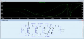
I've included five LTspice simulations of these various capacitances placed in what may (hopefully) be realistic component & circuitry values. The reason why there are five simulations, and not three, is that I've also included:
- a simulation of a single 22nF capacitor placed in the same circuitry - this capacitor value actually seems to amplify the PSU noise with a peak of appr. 18 dBs at 14 MHz ...
- a simulation of two 100 nF capacitors placed in parallel. Something that does not seem to alter the lowest impedance much.
The "digital IC" that is decoupled is the current source I1. The digital IC's package is akin to a QFN or 28 lead SSOP package, hence a lead inductance around ~1 nH to 2.2 nH. I hope this makes for simulations that can be used for this purpose ...
Please note that there are many more capacitors in the simulations than just the ones related to the three options above. I've been trying out various values and decided to let the larger values be in the circuitries since they do not really affect the simulations with respect to resonance peaks & dips.
So what I've been wondering about is:
- Which of these decoupling methods are most effective in technical terms, i.e. they provide the best practical/real world attenuation of digital PSU noise? Is there a generally acknowledged best practice in this field?
- Is there any knowledge about how a particular digital decoupling - and a factual noise spectrum related to this decoupling - correlates with listening impressions?
- Is there a direct and reliable way of measuring - i.e. in a particular circuit - how effective a given decoupling really is? That is: How is it possible to make a reliable measurement in a way that does not interfere with the circuitry - using equipment that is accessible to a DIY'er?
To this end I (with help) designed & built this circuit a couple of years ago:
http://www.diyaudio.com/forums/equi...ier-my-oscilloscope-probes-4.html#post3588959
... with the aim of amplifying the PSU noise and then using my oscilloscope's FFT analysis to display the noise of the PSU. The circuitry works, however, has somewhat more self-noise than is feasible - so I am currently looking for a better solution (i.e. a combination of amplification & low self-noise suitable as an oscilloscope front-end 😛) that is also accessible at a not too high price point. I've been thinking about something like the ERA-3M+ (inspired by a previous 1audio suggestion) with a good PCB layout:
Mini-Circuits
Price-wise accessible. Yet, maybe there are better and still accessible solutions ... ?
Well, no further comments - I hope there'll be some interest in sharing knowledge and practical experiences in this field.
Cheers 😉
Jesper
Hi All,
I have for some time now been reading about digital decoupling and it seems that there are at least three different philosophies about how to optimally decouple digital circuitry. Generally speaking these appear to be:
1. To use one or more capacitors of the same (low) value to provide a low impedance dip where the main decoupling frequency is desired. Could e.g. be one or more 100 nF capacitors to decouple around 12.3 MHz (192 kHz - 32 bits - 2 channels).
2. To use one large(r) capacitor, e.g. somewhere between 1uF to 10 uF, which - in a practical circuitry with PCB (& other) inductances and impedances - gives a lower resonance frequency and fewer impedance dips and peaks. Yet also typically a higher impedance, i.e. less effective filtering, at the desired filtering frequency (for example at 12.3 MHz for a 192 kHz clock).
3. To use a selection of capacitors spaced e.g. 10x values apart, e.g. 100 nF parallelled with 1 uF & 10 uF & 100 uF etc.
I've included five LTspice simulations of these various capacitances placed in what may (hopefully) be realistic component & circuitry values. The reason why there are five simulations, and not three, is that I've also included:
- a simulation of a single 22nF capacitor placed in the same circuitry - this capacitor value actually seems to amplify the PSU noise with a peak of appr. 18 dBs at 14 MHz ...
- a simulation of two 100 nF capacitors placed in parallel. Something that does not seem to alter the lowest impedance much.
The "digital IC" that is decoupled is the current source I1. The digital IC's package is akin to a QFN or 28 lead SSOP package, hence a lead inductance around ~1 nH to 2.2 nH. I hope this makes for simulations that can be used for this purpose ...
Please note that there are many more capacitors in the simulations than just the ones related to the three options above. I've been trying out various values and decided to let the larger values be in the circuitries since they do not really affect the simulations with respect to resonance peaks & dips.
So what I've been wondering about is:
- Which of these decoupling methods are most effective in technical terms, i.e. they provide the best practical/real world attenuation of digital PSU noise? Is there a generally acknowledged best practice in this field?
- Is there any knowledge about how a particular digital decoupling - and a factual noise spectrum related to this decoupling - correlates with listening impressions?
- Is there a direct and reliable way of measuring - i.e. in a particular circuit - how effective a given decoupling really is? That is: How is it possible to make a reliable measurement in a way that does not interfere with the circuitry - using equipment that is accessible to a DIY'er?
To this end I (with help) designed & built this circuit a couple of years ago:
http://www.diyaudio.com/forums/equi...ier-my-oscilloscope-probes-4.html#post3588959
... with the aim of amplifying the PSU noise and then using my oscilloscope's FFT analysis to display the noise of the PSU. The circuitry works, however, has somewhat more self-noise than is feasible - so I am currently looking for a better solution (i.e. a combination of amplification & low self-noise suitable as an oscilloscope front-end 😛) that is also accessible at a not too high price point. I've been thinking about something like the ERA-3M+ (inspired by a previous 1audio suggestion) with a good PCB layout:
Mini-Circuits
Price-wise accessible. Yet, maybe there are better and still accessible solutions ... ?
Well, no further comments - I hope there'll be some interest in sharing knowledge and practical experiences in this field.
Cheers 😉
Jesper
Attachments


Major manufacturers including Philips and Sony use a 100nF capacitor on the chip feed leads, next to the chip. Why make life complicated with a series of capacitors and imaginary inductors when there is no need.
Run separate grounds for digital and analogue then decouple as you go at each digital IC.
Run separate grounds for digital and analogue then decouple as you go at each digital IC.
Hi All,
1. To use one or more capacitors of the same (low) value to provide a low impedance dip where the main decoupling frequency is desired. Could e.g. be one or more 100 nF capacitors to decouple around 12.3 MHz (192 kHz - 32 bits - 2 channels).
Jesper
Same value decoupling capacitors work best for me... the main decoupling frequency as you call it is in fact what needs to be tackled most in a given application. Good to see people experimenting and trying different things...
Nick
there is lots online analysis of digital decoupling with advanced modeling, measurements
http://www.diyaudio.com/forums/digital-source/161368-digital-decoupling-woes.html#post2088212
and there's no universal answer for how digital ps noise translates to analog audio in all of the various scenarios
http://www.diyaudio.com/forums/digital-source/161368-digital-decoupling-woes.html#post2088212
and there's no universal answer for how digital ps noise translates to analog audio in all of the various scenarios
it seems that there are at least three different philosophies about how to
optimally decouple digital circuitry.
Minimizing stray inductance to the ground plane is the key to decoupling.
Even vias can cause problems. A 10nF can be better than a 100nF in some cases.
Last edited:
Hi all,
& thanks for commenting and suggesting 😉
Reading your comments, however, has led me to the decision that it's now time to be able to somehow measure the noise directly/measure the spectrum of the PSU noise instead of considering the various theoretical aspects of this. Given all the practical variables I rather doubt I'll be able to simulate my way to what is actually happening in the circuitry anyway.
So I'll continue along the ERA-3M+ for an active probe and then I'll start out by using my oscilloscope's FFT function and the AD7760 evaluation board (for lower than 1.25 MHz noise).
Should either of you have a better suggestion for an active probe than the ERA-3M+ I'd appreciate hearing about it (maybe having a higher input impedance? DC - ~500 MHz) ... Should still be accessible price-wise 🙄
@jcx: Thanks for the links. I have skimmed and read the texts this morning and e.g. the information on measuring PSU noise in the Xilinx text was very helpful. I imagined it would be so - but fine to have it confirmed.
Cheers from Denmark,
Jesper
Last edited:
Use the smallest package capacitor for the chosen value, 0402 0.1uf is a good choice, preferably with via in pad. Though 0603's would probably do. Placement of vias and number of vias per pin helps, as well as a trace that is wide. The placement of vias in relationship to the cap and ICs pins can also have an effect.
A contiguous ground plane is a must, and preferably a ground/power plane pair would give the best results closely coupled (0.1mm dialectric).
A circuit and more information would be a good idea.
Using through hole capacitors is a total waste of time as any stray inductance is BAD.
Use X7Rs for decoupling....
You really need something like this to work out what is going on:
CADSTAR Power Integrity Advance
We only use it for really serious jobs, for everyday stuff just use experience, put up more info and I can advise further....
http://www.pcbcarolina.com/images/01_PCB_Power_Decoupling_Myths_Debunked.pdf
Decoupling
http://www.ewh.ieee.org/r4/se_michigan/emcs/DL-ARCH-decoupling3.pdf
http://web.mst.edu/~jfan/slides/Archambeault1.pdf
http://www.ece.rochester.edu/users/friedman/papers/TVLSI_06_Decap.pdf
There are other effects on digital circuitry noise levels as well.... again these can be specific to a design...
Hi all,
& thanks for commenting and suggesting 😉
Reading your comments, however, has led me to the decision that it's now time to be able to somehow measure the noise directly/measure the spectrum of the PSU noise instead of considering the various theoretical aspects of this.
Cheers from Denmark,
Jesper
Your focus is on the PSU at the moment because you simulate too much.... The problem is in fact related to the signals carrying high frequency switching signals. Good start would be to consider digital circuits that require 3.3V Vcc supply - not 5. Oscillators are bad, the uCPU are the worst. Preventing this noise from contaminating analog side is very important. You will have to measure this noise on the actual circuit that should be "processing" the signals at the most desired rate. Then, you can see what capacitor values will work best. The amount of noise you have at the analog ground will directly be proportionate to the quality of sound and its ability to give you headaches... or NOT. Also - there's no point in having a "correct" value, position, package and whatnot of the decoupling capacitor, if the ground plane is noisy. Not much of a "decoupling" can happen in that case... so, one must start with a correct ground plane design and then move forward.
Regards,
Nick
Nick
A decoupling capacitor next to a digital IC power pin is there to provide the almost instantaneous requirement for power, it is a very small very fast power supply for when the device is switching...
The sequence of power supply to a switching digital IC is:
On die capacitance
Power plane pair capacitance (closely coupled power and ground pairs are a must)
Local decoupling capacitors
Larger reservoir capacitors
Power supply
Ground planes by their nature are not calm, they are awash with return currents and some switching noise...
There is plenty of information on mixed signal design, there are ways of doing the layouts and interconnectivity that will minimise any effect from one section to another, these are expensive to do though requiring multi layer PCBs, but the same can be done on a more DIY level with care and consideration.
The whole design has to be considered, decoupling is just a part (important) of the whole picture.
Hi Nick & marce ...
Thank you both for commenting 🙂
@ Nick:
Hmmm ... many interesting & relevant comments in your post. I quoted the sentence above because this is my current "challenge" - i.e. how to measure what is actually going on? I'm considering a spectrum analyzer but the price for the ones I've found, and also my guess that they average many samples (and thus may hide semi-random noise), their reduced bit-depth etc. is a reservation on my side ... I don't mind measuring equipment but would like to keep it to a minimum - that which is most relevant. Maybe a high-resolution analog oscilloscope would be a better choice ... ?
So somehow I hope someone in the forums may suggest a suitable probe - or I may have to design one myself.
@marce:
Yup, similar thoughts on my side. Challenging though - I reckon chess players - who learn the principles of PCB layout - could be quite good PCB designers 🙄
Well, thanks again for your comments & suggestions - have a good evening 😉
Jesper
A P.S.: I will post an image of part of the PCB layout tomorrow. If you are so inclined I'd be most interested in hearing how you'd route the clock & data signals. Cheers, Jesper
Thank you both for commenting 🙂
@ Nick:
You will have to measure this noise on the actual circuit that should be "processing" the signals at the most desired rate.
Hmmm ... many interesting & relevant comments in your post. I quoted the sentence above because this is my current "challenge" - i.e. how to measure what is actually going on? I'm considering a spectrum analyzer but the price for the ones I've found, and also my guess that they average many samples (and thus may hide semi-random noise), their reduced bit-depth etc. is a reservation on my side ... I don't mind measuring equipment but would like to keep it to a minimum - that which is most relevant. Maybe a high-resolution analog oscilloscope would be a better choice ... ?
So somehow I hope someone in the forums may suggest a suitable probe - or I may have to design one myself.
@marce:
Yes, that's what's been simmering my mind as well. And I reckon that the return currents through the ground plane - although considered "contiguous" and "same" voltage level - may also radiate into the components and traces nearby ... Writing this I remember an illustration in Henry Ott's book showing exactly this.Ground planes by their nature are not calm, they are awash with return currents and some switching noise...
but the same can be done on a more DIY level with care and consideration.
The whole design has to be considered, decoupling is just a part (important) of the whole picture.
Yup, similar thoughts on my side. Challenging though - I reckon chess players - who learn the principles of PCB layout - could be quite good PCB designers 🙄
Well, thanks again for your comments & suggestions - have a good evening 😉
Jesper
A P.S.: I will post an image of part of the PCB layout tomorrow. If you are so inclined I'd be most interested in hearing how you'd route the clock & data signals. Cheers, Jesper
Yes, that's what's been simmering my mind as well. And I reckon that the return currents through the ground plane - although considered "contiguous" and "same" voltage level - may also radiate into the components and traces nearby ... Writing this I remember an illustration in Henry Ott's book showing exactly this.
You cannot do a digital layout without a ground plane and preferably a few... A contiguous ground plane or voltage plane next to a signal provides the best return path for the ultimate low noise a must, preferably sandwiched between its switching voltage and its ground.
clock as short as possible, any derived clocks again as short as possible and where possible 3X the normal trace to trace clearance... (0.1mm and 0.3mm on many boards these days🙂).I'd be most interested in hearing how you'd route the clock & data signals
Last edited:
@marce:
Thanks again for your comments and suggestions, Marc. Actually, this sentence of yours:
... made me re-layout the PCB - and I think it got quite a bit better. Clocks are now as short as practically possible and they have a ground layer next to them while not really being able to interfere with the rest of the circuitry. Looks fine I think 🙂
So thanks again 😉
Jesper
A contiguous ground plane or voltage plane next to a signal provides the best return path for the ultimate low noise
Thanks again for your comments and suggestions, Marc. Actually, this sentence of yours:
clock as short as possible, any derived clocks again as short as possible and where possible 3X the normal trace to trace clearance... (0.1mm and 0.3mm on many boards these days)
... made me re-layout the PCB - and I think it got quite a bit better. Clocks are now as short as practically possible and they have a ground layer next to them while not really being able to interfere with the rest of the circuitry. Looks fine I think 🙂
So thanks again 😉
Jesper
- Status
- Not open for further replies.
- Home
- Source & Line
- Digital Line Level
- Digital decoupling - its audible & technical effects and possible design solutions?