Dear diyaudio members
It´s been a few weeks i try to repair one audio amplifier. Special one for me, because of these keywords: cascoded current mirrors, fully symmetrical design, direct coupled with DC-servo. Voltage feedback is taken from the "darlington driver" stage which drives the IGBTs and for zero DC output is responsible the only not discrete component on the board - the OP07.
The main problem was "invisible" but while checking with the scope I found the problem in defective via in PCB under one of the main caps pins. This cap filtered the -56V rail. The result was overloaded power stage. This was audible while turning on the machine. The logic board watched this status carefully and immediately disconnected this faulty channel off. After this procedure I powered the amp again but another issue appeared. Voltages on gates of power IGBT´s are not symmetric for N and P and also it is impossible to set any quiescent current thru output transistors. The "thermal sensing" BD139 which is responsible for idle current setting doesn´t allow to open them.
I already soldered out these nice Toshiba IGBTs and measured gate treshold voltages and these sits around 2,5V.
The problem is that whole output from the input module is DC shifted and I could not find any way to set this correctly.
The input module was small PCB completely sealed in plastic enclosure with 10pin board to board connector. In the schematic this module is highlited as INPUT MODULE. The manufacturer of this amp wasn´t much helpful so I made some cruel reverse engineering and redrawn the full schematic of power amplifier board.
1: repaired faulty via in PCB
2: checked output transistors and I also measured them on curvetracer
3: checked OP07, it was good, but replaced with new one
4: found some BC550/560´s with very low beta(can´t remember which exactly)
5: paired and combined the transistors to match positive/negative 15 and 16V rails
6: paired transistors in outer current mirrors which are biasing the input transistors inside input module
7: the same was done for inner cascoded current mirrors
Pairing was in a sense of chooding the Vbe, h21e and reverse biased EB breakdown. I played with everything at this board but there is still assymetry on input module outputs..I gave up and posted this thread. Any advices ladies and gentlemen?
Attachments

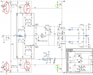
In the red circles circuits that appear curious to me - I'd expect something as in the green circles. Can you measure the voltages there just to be sure?
And also the voltages indicated with the cyan circles - that might give a clue where things go wrong. Bias is +3.20 and -2.34 but can be normal to compensate for differences in the P/N igbt's; the midpoint voltage between the drivers is ok with given bias of 5.54Vdc. What's the value of the BE resistor of the BD139?
And also the voltages indicated with the cyan circles - that might give a clue where things go wrong. Bias is +3.20 and -2.34 but can be normal to compensate for differences in the P/N igbt's; the midpoint voltage between the drivers is ok with given bias of 5.54Vdc. What's the value of the BE resistor of the BD139?
Attachments
Sorry, There is a mistake in schematic at +16V rail. There are also the NPN devices used. The reverse biased EB junction acts like a zener diode. You can measure 7-8V on it. The +/-16V rails are the almost same within 50mV.. Voltage on positive Gate of output transistor is around 2,0V..negative Gate sits at 1,2V. BE resistor of BD139 is 953 Ohm. I will upload corrected schematic tomorrow with component names also to be more clear.
Hello, I attach corrected schematic. I also added test points as they are on original PCB. Accidentaly multimeter tip fell down on PCB and made next fault.
In respect to GND we took voltages as follows:
TP1= 0,41V
TP2=15,61V TP3=-15,40V TP4=16,68 TP5=-16,20V
TP6=3,48V TP7=-2,24V TP8=2,29 TP9=-1,53V
TP10= 50,8V TP11=-50,9V
Voltage between +in and -in on the input module was around 25mV as i remember.
Difference between TP7 and TP9 is indicating something went wrong. But Transistors Q29 and Q30 aren´t in short. But I must take them out and check.
I actually forget to mention, that on main PCB there is also another PCB module which monitors the clipping, heatsink temperature, current thru output transistors. It steals signal from 0,22R emitter resistors of output transistors via 680R resistor. On this board there is LM324 and it gets pretty warm. Also voltage regulator which supplies it is damn hot. Maybe the problem is in the protection circuit itself..
Attachments

Protection board has nothing to do with overall function of the main board, so i let the amp on to heat up and take again some measurement:
TP1 0,49V
TP2 15,67V TP3 -15,44V TP4 17,10V TP5 -16,21V TP10 50,2V TP11 -50,2V
TP6 3,44V TP7 -2,67V
TP8 2,26V TP9 -1,50V - maximum possible values. Can´t go further. It´s like Q11 is too much open. But, when i moved it on the breadboard, it was easy to set the Vce from 1V to 13V without any problem(Ice was in range of mA)..this is the reason i think Q11 is OK and the problem must be somewhere else. Maybe beta of transistors in cascoded current mirrors is critical and should be at some minimum value. Any ideas appreciated!
Voltages TP8/TP9 are basically TP6/TP7 minus 2x Vbe of Q9+Q10, resp Q29+Q30.
So everything works as before, 0V DC offset on output but +400-500mV DC on the node between R9 and R10..
I attach also characteristic of power output transistors. Still can´t set necessary voltage span to open the gates..
Attachments


zener d6 is not well or shorted/shorting, replace; Vmax TP7 is now set by D6
edit: didn't see your #6 while analysing...
edit: didn't see your #6 while analysing...

- Home
- Amplifiers
- Solid State
- Direct coupled amplifier problem