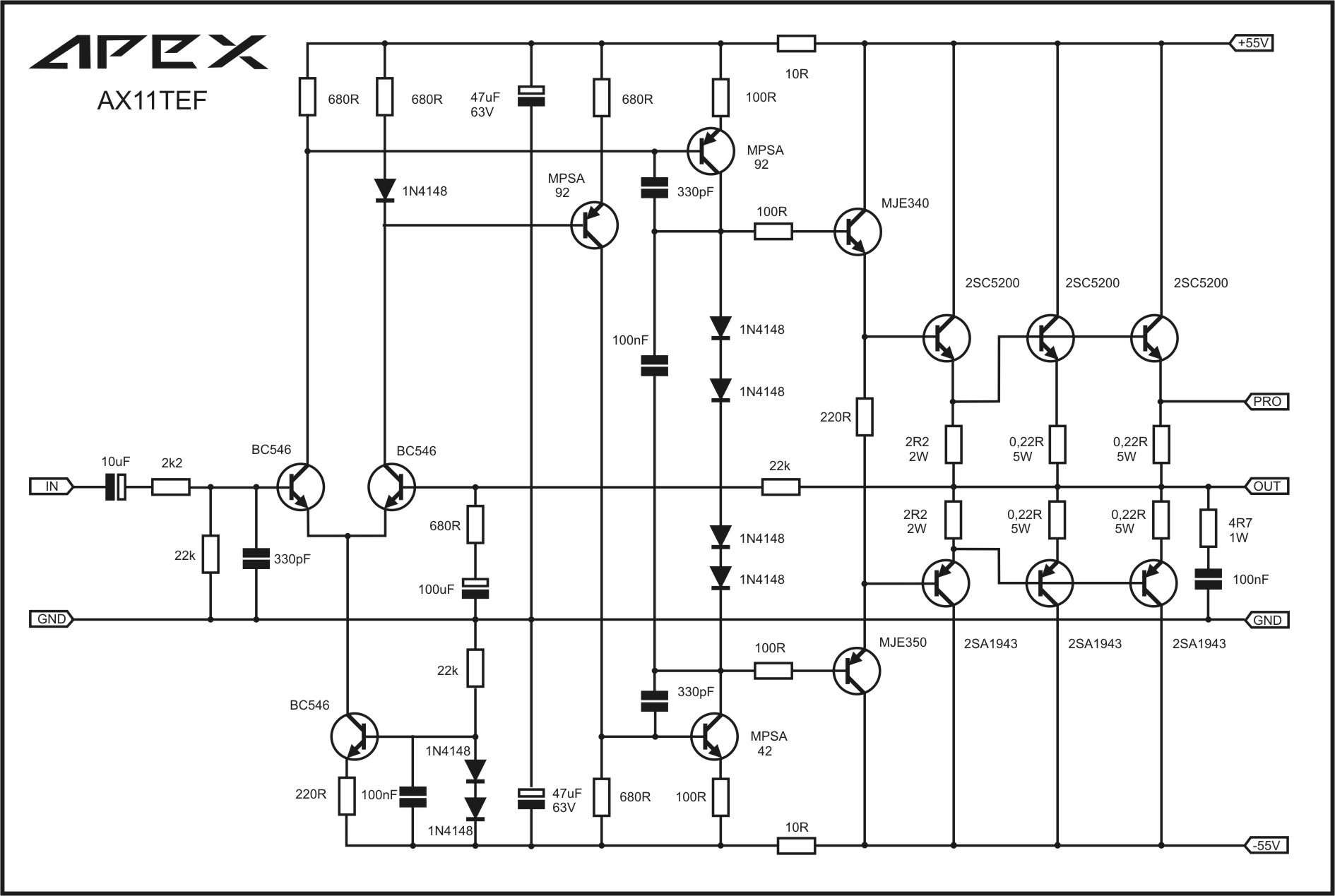
AX11TEF from apex for example. On the base of the outputs how do I figure the base voltage. I have a good understanding of most of the circuts after 3 years of studying electronics. But when I see for example 50V plus rails and the output transistors bases connected to the collector of the predrivers it seems that the voltage will be way over 5v. I know i am missing some very important point, im sure a very basic mistake in reading the schematic or understanding the base voltage. If i can just grasp this i think it will clear up a massive problem i have in designing circuts. I have no problems with base biased circuts that involve only a few transistors and a resistor divider network. But I cant seem to grasp this biasing in the output sections
Last edited:
You can estimate all the voltages in a circuit like this...
Lets assume the circuit is functioning normally and there is zero volts DC offset.
The collector voltage of the predrivers as you call them will be around +1.8 volts on the upper PNP device and around -1.8 volts on the lower NPN.
Can you see how that quick estimation is derived ?
Lets assume the circuit is functioning normally and there is zero volts DC offset.
The collector voltage of the predrivers as you call them will be around +1.8 volts on the upper PNP device and around -1.8 volts on the lower NPN.
Can you see how that quick estimation is derived ?
I think my problem is a poor understanding of max base voltage. I see a large ac voltage swing at the base on output 2sc5200 after emitter of mje340 VAS which seems to blow away the 5v max. So i also have a poor grasp on the ac portion also. I just saw you response so i will think on that for a few
I get that for the mpsa 42/92 . Is that what you mean. But I get lost on the mje340 to 2sc5200 base. I can only see a big voltage hitting the base of 2sc5200 from mje340. And i know thats wrong of me.
The output stage is biased via 220 ohm's resistor in MJE340/350 emitter.
And the voltage across this resistor is "set" by this four 1N4148 diodes.
From KVL we have:
4*0.7V = Vbe_MJE340 + I*220R + Vbe_MJE350 (I ignore the base current).
Hence the MJE BJT's current will be around
I = (4*0.7V - 2*0.7V)/220R = 6.3mA
And from the output stage, we can write this KVL
I*220R = Vbe_2500 + Ie*2.2R + Ie*2.2 + Vbe_1940
1.4V = Vbe + Ie*2.2R + Ie*2.2 + Vbe
But we cannot solve this analytically because we do not know the BJT's parameters.
And for every single BJT's, we will get a different result.
But what we can tell is that this current will not be larger than
Ie = (1.4V - 2*0.4V)/4.4R = 140mA ( I assumed the output stage BJT's Vbe_min is 0.4V).
And the last four BJT's (with 0.22R at emitter) will be cut-off.
Ok, Thank you sirs. I will digest this for the day and see if I can grasp it. Has been hard from books alone. But this is starting to add up for me
I think my problem is a poor understanding of max base voltage. I see a large ac voltage swing at the base on output 2sc5200 after emitter of mje340 VAS which seems to blow away the 5v max. So i also have a poor grasp on the ac portion also. I just saw you response so i will think on that for a few
The base voltage can be 'any' value... so lets explain that simply...
Firstly, a silicon transistor such as all these will develop or 'drop' around 0.6 to 0.7 volts across the base-emitter junction when forward biased. In a circuit like this we never reverse bias any of the junctions.
The NPN's will always have the base at around +0.6 relative to the emitter.
The PNP's will always have the base at around -0.6 relative to the emitter.
So the as the AC signal rises on the collector of the MPSA92 the emitter of the MJE340 will follow that signal less 0.6 volts. The emitter of the 2SC5200 driver does the same less another 0.6 volts with the same happening again at the final output.
So we can have 30 volts applied to the base of the MJE340 and we would see around 28.2 on the emitter of the output.
The PNP half does the same but with opposite polarity signals, that is those signals that are negative relative to ground.


I think the mystery is in assumed 5v max base voltage. It's a junction thing in ratio, base/emitter etc..

Thank you Mooly , that cleared up my issue with ac swing around the base. And Jony thank you for clearing up my DC opp point issue. I guess I needed to hear it again only from a diff perspective.
- Status
- Not open for further replies.
- Home
- Amplifiers
- Solid State
- Help understanding base voltage