Greetings everyone.
I'm requesting some assistance with the design of a current limit circuit that is all but working save for a final element that I'm adding but it's not behaving as expected. The addition of Q9 is my area of focus. It's causing unexpected behavior around the circuit that has behaved as expected prior to its addition.
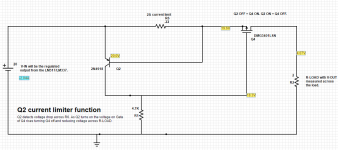
In image 2 current limiting is active. Q2 senses the v-drop across the in-circuit current limiting resistor in series with the ON state of Q6 with negligible ON resistance. Without Q9, Q2 Collector happily toggles between 0v (when OFF) and 12v (when ON). I want to use this voltage swing to turn Q9 ON & OFF to control Q3 and ultimately Q4.
BUT, adding Q9 is suppressing the ON state of Q2 as can be seen in image 2. I find that odd because I would have expected the large input impedance Gate/Source of Q9 to not affect the action of Q2. But it is and as a result Q9 is not properly switching Q3 ON to turn OFF Q4 fully which is the ultimate goal of the current limiting function.
Another oddity since the addition of Q9 is that the v-drop to turn on Q9 never fully develops to 0.6/0.7v as it does without Q9 in circuit. So this now isn't behaving correctly either.
I have tried different types of N-CH MOSFETS to see if the characteristics of another MOSFET would help but no joy. Fundamentally there's design flaw here I think.
Extra background: I recently added Q9, Q3 & R5 to fully switch OFF Q4 when limiting is active. Previously I had the collector of Q2 connected to the gate of Q4 but this design never fully switched off Q4.
Note re components shown
Q4-8 are IRFR-5305 P-CH enhancement mode MOSFETs (working nicely in circuit)
Q2 is 2N2905A (working nicely in-circuit)
Q9 & Q3, R5 & R10 are Partsim experimental components only at this stage for modification testing
If someone can suggest what's going wrong here I'd appreciate the feedback. I'm trying to keep this simple to minimise PCB real estate.
Thanks,
Steve
I'm requesting some assistance with the design of a current limit circuit that is all but working save for a final element that I'm adding but it's not behaving as expected. The addition of Q9 is my area of focus. It's causing unexpected behavior around the circuit that has behaved as expected prior to its addition.
In image 2 current limiting is active. Q2 senses the v-drop across the in-circuit current limiting resistor in series with the ON state of Q6 with negligible ON resistance. Without Q9, Q2 Collector happily toggles between 0v (when OFF) and 12v (when ON). I want to use this voltage swing to turn Q9 ON & OFF to control Q3 and ultimately Q4.
BUT, adding Q9 is suppressing the ON state of Q2 as can be seen in image 2. I find that odd because I would have expected the large input impedance Gate/Source of Q9 to not affect the action of Q2. But it is and as a result Q9 is not properly switching Q3 ON to turn OFF Q4 fully which is the ultimate goal of the current limiting function.
Another oddity since the addition of Q9 is that the v-drop to turn on Q9 never fully develops to 0.6/0.7v as it does without Q9 in circuit. So this now isn't behaving correctly either.
I have tried different types of N-CH MOSFETS to see if the characteristics of another MOSFET would help but no joy. Fundamentally there's design flaw here I think.
Extra background: I recently added Q9, Q3 & R5 to fully switch OFF Q4 when limiting is active. Previously I had the collector of Q2 connected to the gate of Q4 but this design never fully switched off Q4.
Note re components shown
Q4-8 are IRFR-5305 P-CH enhancement mode MOSFETs (working nicely in circuit)
Q2 is 2N2905A (working nicely in-circuit)
Q9 & Q3, R5 & R10 are Partsim experimental components only at this stage for modification testing
If someone can suggest what's going wrong here I'd appreciate the feedback. I'm trying to keep this simple to minimise PCB real estate.
Thanks,
Steve
Attachments


It's not a bistable circuit.As long as Q2 does nothing the output is a voltage source with Rseries as source resistance.From the moment Q2 commes alive the output is a (not so good) current source, it doesn't turn off, the output voltage depends on the load.The rest adapts there voltages to get that (~stable) current, changes with the load.
Mona
Mona
If someone can suggest what's going wrong here I'd appreciate the feedback.
What exactly are you trying to achieve?
The circuit looks hugely overcomplicated and nonsensical, and will probably never work satisfactorily in reality.
There are much simpler ways of making a current limiter
Thanks for the replies.
Here is a simplified example of the problem to clarify what I'm trying to achieve.
Essentially this is representing a current limiting circuit to control the output of a variable 0-30v power supply. R2 represents where the variable output would have the load attached to.
The problem to solve is turning Q4 OFF entirely which the existing design is not achieving 100%. I need to get the gate voltage on Q4 much closer to its source voltage to achieve this.
I hope that's much clearer.
Steve
Attachments
If Q4 is turned off there is no current in the load no more.You have to hold the condition and have a means to turn the circuit on again.
Mona
Mona
Hi Ketje,
Thank you for your reply.
R2 is just representing "a device under test" connected to the output of this benchtop variable PSU.
If the device under test triggered the current limit - then the device would be disconnected, Q4 would turn back on and full voltage would be restored.
I have attached a further simplified illustration.
The challenge is to find the discreet components to add between Q2 & Q4 to achieve 100% switch off of Q4 under full current load.
Thanks,
Steve
Attachments

By your circuit I assume that you have little or no understanding about how to do custom amplification stages with transistors and achieve frequency stability with compensation.
A TL07x can sense voltage up to half a diode drop above positive rail. A LM358 can sense voltage down to half a diode drop below negative rail. These chips exist for a reason. I recommend doing the circuit with an op-amp and a FET, with resistor-zener supply as needed to limit supply voltage to op-amp, and finding suitable frequency compensation for stability, which would need a small value C (or RC) as a minimum dummy load, and another RC in the op-amp. An output reversal diode is also recommended if the load can become inductive. The current limit can be adjusted by switching the reference voltage fed to the op-amp.
A TL07x can sense voltage up to half a diode drop above positive rail. A LM358 can sense voltage down to half a diode drop below negative rail. These chips exist for a reason. I recommend doing the circuit with an op-amp and a FET, with resistor-zener supply as needed to limit supply voltage to op-amp, and finding suitable frequency compensation for stability, which would need a small value C (or RC) as a minimum dummy load, and another RC in the op-amp. An output reversal diode is also recommended if the load can become inductive. The current limit can be adjusted by switching the reference voltage fed to the op-amp.
Thank you for that feedback Eva - noted.
I appreciate that the method represented here is very basic and that there are many other ways to solve the problem. I decided to keep the design very simple and it was possible to test on the simulator.
I will look into what you've suggested.
I appreciate that the method represented here is very basic and that there are many other ways to solve the problem. I decided to keep the design very simple and it was possible to test on the simulator.
I will look into what you've suggested.
If you want to keep your (not very good) method, here is the way to do it:
Instead of a transistor, you can use a small SCR as a sense element.
Since you place your circuit in the positive rail, the SCR has to be a P-gate, or as in this case a thyristor-tetrode of which you use only the anode gate.
Note that a SCR can be emulated with two transistors and two resistors.
The best solution however is to follow Eva's advice, and even better, to integrate the limiter in the upstream supply: you already have a pass element, you just need to control it according to current in addition to tension.
That's what is done is all lab supplies
Edit:
With an input reaching up to 30V, it is prudent to add a 15V zener between the gate and the source of the PMOS, to avoid stressing its gate excessively
Attachments

Last edited:
That's very useful as an option Elvee and much appreciated.
I'll have a good look at that.
Thank you.
I'll have a good look at that.
Thank you.
This is a sample circuit of high-side adjustable current regulator with foldback. Component values are a first guess, the schematic needs some work figuring out optimum values, but the topology is right.
EDIT: The circuit does have a problem: the output of current sense TL072 does not swing to +Vcc, but it may do with a 1k resistor, or using 2-3 diodes to move the IN+ reference 1.2~1.8V down. A diode is required in series with collector of foldback sense transistor to avoid the effect reversing when the transistor saturates. Anyway the circuit illustrates the linear power supply principles intended to be shown: Adjustability, linear operation, minimum load at HF for stability, and foldback protection.
EDIT: The circuit does have a problem: the output of current sense TL072 does not swing to +Vcc, but it may do with a 1k resistor, or using 2-3 diodes to move the IN+ reference 1.2~1.8V down. A diode is required in series with collector of foldback sense transistor to avoid the effect reversing when the transistor saturates. Anyway the circuit illustrates the linear power supply principles intended to be shown: Adjustability, linear operation, minimum load at HF for stability, and foldback protection.
Attachments

Last edited:
- Status
- Not open for further replies.
- Home
- Amplifiers
- Power Supplies
- Help with current limiting MOSFET circuit design