Hi,
I have a NOS Dac in passive so it doesn't have inverting output.
Read somewhere need a hex inverter prior to the dac.
Is it just case of putting DIR9001 output into the 'flat' side of triangle (in the diagram) and output to DAC? The Hex inverter is powered / tapped from another local inverter that has no spare gates.
Is this right?
Attachments

Last edited:
Update, there is sound now... but I'm still unsure if I connected it up right... with regards to the triangle.
Yes, you wire an invertor as you describe. Also you must not leave all the unused inputs floating but should tie them to either ground or supply. So if you used invertor number 1 (pins 1 and 2) then you can easily link pins 14,13 11 and 9 and pins 3, 5 and 7.
If this is outputting SPDIF then that should as far as I recall be polarity independent. Maybe the levels were marginal and the invertor has brought them up. You can also parallel two or more invertors to get more current drive.
If this is outputting SPDIF then that should as far as I recall be polarity independent. Maybe the levels were marginal and the invertor has brought them up. You can also parallel two or more invertors to get more current drive.
This solution should work, but the inverter will introduce a delay of several ns to the signal. So your data line will be delayed by a few ns compared to the other signal lines.
If I were you, just to be on the safe side, I'd use a D type flip-flop to reclock all signals before feeding them to the DAC chip(s).
Unless you know that your DAC chip(s) already do that internally.
If I were you, just to be on the safe side, I'd use a D type flip-flop to reclock all signals before feeding them to the DAC chip(s).
Unless you know that your DAC chip(s) already do that internally.
Hi, the DAC is TDA1543, no internal reclock, but the DIR9001 probably does?
Would it perhaps be better to put the inverter at SPDIF side...
If not do you have a schematic available?
I am familiar with flip flop re-sync. They can be used in place of the SAA7220 DF before the 1541 to reclock signals for example, pre-made ones exist on ebay for £20 but this is far too expensive! I've been meaning to ask for a schematic for a long time... that price isn't justifyable IMO!
Last edited:
It is my understanding that ladder dac are more tolerant of jitter than ones that utilize oversampling, the jitter translates into INL (wave squash) which isn't too subjectively objectionable (harmonic distortion).
The DIR9001 does some de-jittering on the s/pdif signal, but what it outputs will need de-jittering before it enters the DAC chip.
If you put the inverter at the s/pdif side, all you'll manage is to harm the s/pdif signal. If the DIR9001 manages to lock into the signal, it will still output a signal that will need inverting.
The reclocking circuit is very simple, all you need is a D type flip-flop, but the more crucial part is the selection of the actual flip flop plus the implementation.
I've used single flip-flops with good results (like the 74AUP1G79) but Potato Semi parts are supposed to be better.
But the actual layout of the PCB is also important, like the trace lengths, the trace impedances, the power supplies, the decoupling, etc.
Do you have a schematic of your current implementation? Just the digital part..
I don't but the input to the 1543 are pretty self-evident.
Its the Muse TDA x4 Parallel Dac.
Its the Muse TDA x4 Parallel Dac.
Attachments

Last edited:
I just re-read your first post and it seems that I misunderstood your original question.
I see that the TDA1543 accepts normal I2S signal.
So, what are you trying to achieve with the inverter?
What do you mean by "..it doesn't have inverting output"? What exactly are you trying to do?
I see that the TDA1543 accepts normal I2S signal.
So, what are you trying to achieve with the inverter?
What do you mean by "..it doesn't have inverting output"? What exactly are you trying to do?
As there is no op amp with inverting output, the polarity at DAC analog out is incorrect polarity.
The data line flip is needed and is a solution I read by abraxalito, a user here on diyaudio. 🙂
The data line flip is needed and is a solution I read by abraxalito, a user here on diyaudio. 🙂
As there is no op amp with inverting output, the polarity at DAC analog out is incorrect polarity.
The data line flip is needed and is a solution I read by abraxalito, a user here on diyaudio. 🙂
This raises an interesting question, as I just looked at the TDA1543's data sheet and didn't note any mention of the output signal's polarity. So, it may or may not be correct to invert the data signal. Assuming that it's correct to invert the data, inserting an inverter gate in the I2S data line between the DIR and the DAC, while not totally accurate, works fine in practice. The additional few nanoseconds of data signal skew due to the propogation delay of the inverter gate will be totally inconsequential in your intended application. Threre's absolutely no need to be concerned over it.
If your DAC happens be your only signal source, the best and also the easiest solution I can think of is simply to reverse the polarity of the speaker cable connection. Either reverse the cable connection at the amplifier output terminals, or instead at the speaker terminals.
Last edited:
......The additional few nanoseconds of data signal skew due to the propogation delay of the inverter gate will be totally inconsequential in your intended application. Threre's absolutely no need to be concerned over it.
Agreed, but if one wants to be anal about it I would put a similar non-inverting buffer gate in the I2S L/R and CLK lines to even up the delay. Because re-clocking will not fix the timing skew but rather shorten the non-delayed pulses which may cause more harm than just leaving as-is.
Also it's true that SPDIF (and balanced AES) is not polarity sensitive as it's Manchester encoded. But keep in mind the DATA line in I2S is not SPDIF!
Agreed, but if one wants to be anal about it I would put a similar non-inverting buffer gate in the I2S L/R and CLK lines to even up the delay. Because re-clocking will not fix the timing skew but rather shorten the non-delayed pulses which may cause more harm than just leaving as-is.
My point was that a few nanoseconds of timing skew on the data line is not a jitter inducement, not does it provoke data errors. It's totally inconsequential in his application. The data is clocked in to the DAC well away from it's transitions, and well within the hold period of each data bit. Therefore, there's no benefit to reclocking any of the I2S lines due to a few nanoseconds of data signal delay.
Last edited:
Agreed, but if one wants to be anal about it I would put a similar non-inverting buffer gate in the I2S L/R and CLK lines to even up the delay.
Seeing as I've noticed a mention here I do use this approach when I need an inverted data signal. As a single hex inverter tends to bring a whole 14pin package along with it, I use a 74HC86 where the individual gates can be configured to invert or not - the CLK and WS get buffered and the remaining two gates give me true and inverted DATA.
Seeing as I've noticed a mention here I do use this approach when I need an inverted data signal. As a single hex inverter tends to bring a whole 14pin package along with it, I use a 74HC86 where the individual gates can be configured to invert or not - the CLK and WS get buffered and the remaining two gates give me true and inverted DATA.
As Ken said above, it's really not necessary to worry about. But using a 74xx86 is a practical idea in that you can run all three or four I2S lines through it. As with an XOR gate, a high on the opposite input inverts, a low does not.
Me, If not a PC layout hassle I would buffer all the I2S lines through the 74xx86 although again, Ken is right, it's not critical in this application.
Also remember you can make an inverter with an NPN transistor and two resistors. 2N3904, 10K in series to base, 4.7k from VCC to collector, emitter grounded. The inverted signal is on the collector. This avoids the 14pin package although it takes up just as much space and half the number of holes or SMD pads. I like the 74xx86 better!
Last edited:
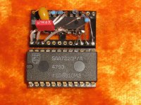
While on the subject does anybody know how this works? It looks like it has 28pins?
Its a reclock as well... I'd be interested in a schematic.
I may use it in another project but I might just use a usb asynchronous Amanero board on its own... I'm confident the necessary measures are employed in the amanero, to do what that 28pin thing otherwise does... (reclocking).
Thanks
Its a reclock as well... I'd be interested in a schematic.
I may use it in another project but I might just use a usb asynchronous Amanero board on its own... I'm confident the necessary measures are employed in the amanero, to do what that 28pin thing otherwise does... (reclocking).
Thanks
Attachments
- Status
- Not open for further replies.
- Home
- Source & Line
- Digital Line Level
- Hex inverter to flip DATA line