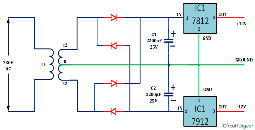
Hi! I come across a highend Japanese amplifier, the power transformer is center tapped, normally we only need to use 4 diode to get the dual supply like the circuit below:
This amplier's dual supply rectifier circuit use 8 diode:
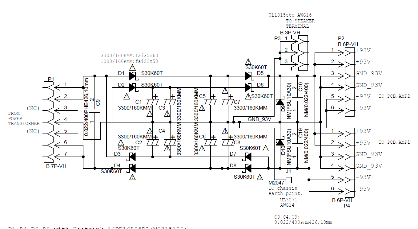
This circuit connected to a 3KW transformer.
May I know what is the benefit of this circuit?
Thanks.
This amplier's dual supply rectifier circuit use 8 diode:
This circuit connected to a 3KW transformer.
May I know what is the benefit of this circuit?
Thanks.
Attachments


Last edited:
Looks like the second one is diode-OR’ing the two individual half wave rectifiers to make a full wave (on each + and -). The diode symbol is a Schottky, which suggests this is a switch mode supply. Maybe it was quieter and had less EMI that way? It would reduce the ripple frequency in the caps by a factor of two. At 60/120 Hz you wouldn’t want this, but at switch mode frequencies one might want to. Offhand I couldn’t think of why, unless it was about reducing high frequency noise.
I think its to reduce the stress on the caps and transformer from charging pulses which only see one capacitor, yet have both caps available to source current during heavy loads - after each charging pulse one cap takes all the current till it dicharges to match the other's voltage - thereafter both caps work together till the next charging pulse.
Not sure it has any real advantage, but might be worth simulating.
It does have some redundancy, any single cap or diode failure (open circuit) can be tolerated.
BTW using schottky diodes at these high voltages is a tricky business, they will easily go into thermal runaway from reverse leakage if not properly heatsinked and kept cool.
Standard circuit will have both diodes connected to filter capacitors. If supply is 50 Hz, the ripple frequency on the capacitors will be 100 Hz. Both loose charge at the 100 Hz rate after passing the peak. In this new design, each capacitor sees only 50 Hz ripple. Each ripple is out of phase to the other set of capacitors. So when set is loosing charge, other will be delivering current. This is what I see. Regards.