Hi. Long time reader, new poster here.
I have been working on a pcb layout for an LM3886 based amplifier that I plan to build. Plan is to go single layer for various reasons. I will be etching my own board. Main concern at this point is the grounding scheme. I know single point/star grounding can prevent a lot of issues. Somewhere along the way I ended up with ground pours.
My expectations right now are to get a board etched to test and get that up and running first before building the final pair of boards. I have some extra lm3886 devices I bought for that and breadboard abuse. I do own a 100MHZ digital scope so I have some ability to look for issues.
Any feedback is greatly appreciated. I do plan to clean up the layout so I am open to implementing suggestions.
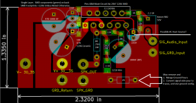

I'm struggling with the ground circuit on my lm3886 board, so have read threads below, maybe this will help:
Some measurements with different ground schemes
http://www.diyaudio.com/forums/chip-amps/252436-lm3886-pcb-vs-point-point-data-3.html#post3846783
pages 19-21 is interesting to read
http://www.diyaudio.com/forums/chip-amps/252436-lm3886-pcb-vs-point-point-data-19.html
Some measurements with different ground schemes
http://www.diyaudio.com/forums/chip-amps/252436-lm3886-pcb-vs-point-point-data-3.html#post3846783
pages 19-21 is interesting to read
http://www.diyaudio.com/forums/chip-amps/252436-lm3886-pcb-vs-point-point-data-19.html
The muting circuit (connected to pin 8) is not correct. According to the LM3886 datasheet your circuit needs to source at least .5mA from pin 8 to turn the muting function off.
What schematic are you following?
What schematic are you following?
Any feedback is greatly appreciated. I do plan to clean up the layout
so I am open to implementing suggestions.
Do you have thermal reliefs for pads that are on the wide foil areas?
If not, soldering those will be difficult.
The polarity of the negative rail capacitors are incorrect. Should have positive connecting to ground.
Mute resistor is missing and I prefer to connect Cm to power ground and not to the input ground.
Speaker return and 2R should/could be closer to the 22uF capacitors (ground).
Add a 100-330nF capacitor at the input.
Mute resistor is missing and I prefer to connect Cm to power ground and not to the input ground.
Speaker return and 2R should/could be closer to the 22uF capacitors (ground).
Add a 100-330nF capacitor at the input.
Last edited:
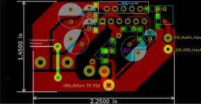
Ok here is another revision. I was able to implement alot of the suggestions, and I will be exploring more in further revisions. I left component values out of the second drawing.
1. Moved ground for mute delay capacitor (CM) to its own ground trace. Took it off the input ground.
2. Fixed polarities of electrolytic caps, that I had ignored previously. I think I got them all, but I will recheck tomorrow.
3. I didn't get a chance to implement thermal reliefs but I may still do this on a few of the pads.
4. Drew (resistor connecting pins 4 and 8) I had previously left this out of the layout since I may solder it right to the pins.
5. Increased the size of the foot print for the output resistor/inductor Changed layout to accommodate this
6. I will explore revising grounding further to get the speaker return closer to the supply bypass caps. That suggestion came after this current revision so I will have to see what I can do in the next.
7. There is a jumper connecting the 2 ground pours, and only after looking at it did I realize there is plenty of room to get rid of it. That will most likely be going away.

Last edited:
Error in my first post (#5). Should be 100-330pF at the input.
I would leave the 2R resistor. You can bridge it if you don't have a ground loop hum problem.
A good way of analyzing the layout is to trace the current loops. Input to input return looks good to me. The power and output loops don't look so good. It maybe difficult to improve with a single sided board.
Error in my first post (#5). Should be 100-330pF at the input.
I would leave the 2R resistor. You can bridge it if you don't have a ground loop hum problem.
A good way of analyzing the layout is to trace the current loops. Input to input return looks good to me. The power and output loops don't look so good. It maybe difficult to improve with a single sided board.
I will add the cap across the input.
I was able to move the speaker, and zobel ground using jumpers, but that still left the pesky mute ground, and the trace for that was getting kind of long. I am going to shift gears and at least try a second layer. Second layer will be kept to a minimum for lack of proper vias, plated through holes, and solder mask. So to say the least it won't be fully utilized but what I have tried so far it cleans things up a lot.
Last edited:
Spent a few days reading the lm3886 point to point discussion between Mark, and Tom and re-reading TomChr's scholarly articles. Mostly learning how much I don't know, but I think I am slowly getting a better grasp.
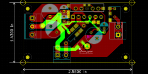
I re-did most of the layout again and got into a second layer. PCB is down to about 1.43" x 2.58"
This time there is about .94" of trace (100 mils wide) between the connector for the load ground return and the via at the decoupling caps. If this grounding scheme is looking better, I will probably redo the traces with larger pours.
I may deviate from the datasheet recommendations for the zobel RC values for more headroom (dissipation) and better component selection. Thinking of something like 8.2R, and 33NF. I can get 8.2R thick film in a 1210 1w part.

Are the lime green traces the only traces on the top side?
I can't see input RF attenuation.
I tried to follow Tomchr explanation of why he connected references to the Speaker Return. But I didn't understand what he was getting at.
What little I did get does not seem to agree with your layout.
I do like the very tight groupings at the power inputs and again for the signal inputs.
Why did you separate the input zero volts from the trace connecting the first two decoupling electros?
I'm not sure what advantages come from the big copper fill attached to the signal return brings.
Last edited:
Are the lime green traces the only traces on the top side?
I can't see input RF attenuation.
I tried to follow Tomchr explanation of why he connected references to the Speaker Return. But I didn't understand what he was getting at.
What little I did get does not seem to agree with your layout.
I do like the very tight groupings at the power inputs and again for the signal inputs.
Why did you separate the input zero volts from the trace connecting the first two decoupling electros?
I'm not sure what advantages come from the big copper fill attached to the signal return brings.
I gather that the main issue with how I returned the ground to the speaker return input is that it only serves to increase loop area beyond what is necessary. The difference being I am not using continuous ground planes.
I take it I should scratch that idea and just return everything separately to a star ground located as close as possible to the decoupling caps, and try to cut down on loop area of the input ground which I haven't really improved much thus far.
RF attenuation will be added in next revision. I assume this is CC (220pf) on the datasheet. I have seen references to putting it across the input, and signal ground rather than the two op amp inputs as called for in the data sheet. I will search the past discussions on this since it seems like it has been discussed in detail before.
I gather that the main issue with how I returned the ground to the speaker return input is that it only serves to increase loop area beyond what is necessary. The difference being I am not using continuous ground planes.
Ground plane or spider ground, the reference ground should connect to the speaker return. It's the voltage across the speaker you're trying to control. With a single ended circuit, connecting the grounds at the speaker return is the best you can do. You can read my rationale here: LM3886 chip amp grounding.
I take it I should scratch that idea and just return everything separately to a star ground located as close as possible to the decoupling caps, and try to cut down on loop area of the input ground which I haven't really improved much thus far.
A star ground or ground spider is the most effective way to shoot yourself in the foot, actually. The best grounding scheme is one that results in the lowest ground impedance (resistance and inductance mainly). A spider ground maximizes the ground impedance. That's not what you want if you're after good performance (or even reproducing the data sheet performance of the LM3886. In addition to minimizing the ground impedance, you need to keep the large currents (supply and speaker return) and dirty currents (feedback return) away from the clean input ground. This can be done either by using separate planes/pours and/or by careful component placement.
You can find my measurements of star ground vs other grounding techniques here: http://www.diyaudio.com/forums/chip-amps/252436-lm3886-pcb-vs-point-point-data.html
You can also find the performance graphs of my implementation of the basic LM3886 circuit (with RF filter and the components needed for good stability) here: LM3886 Done Right
RF attenuation will be added in next revision. I assume this is CC (220pf) on the datasheet.
No. Cc (and associated Rf2 and Cf) combats quasi-oscillation as the output swings near the rails. This is described in the application section of the data sheet. I suggest adding the Zobel and Thiele networks to your circuit if you want good stability.
The layout you show in Post #9 is actually pretty decent. You could just flood the top layer with a ground plane and be almost there.
Tom
Maybe you would publish it on circuitmaker?
Free PCB Design Software | CircuitMaker
I don't know how easy it is to transfer your PCB design from your software to altium, though.
Free PCB Design Software | CircuitMaker
I don't know how easy it is to transfer your PCB design from your software to altium, though.
- Status
- Not open for further replies.
- Home
- Amplifiers
- Chip Amps
- Lm3886 pcb layout