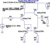
This has probably already been investigated earlier, but I took a fresh look at a low-distortion voltage-follower/buffer, with encouraging results. The main idea is to use a super-pair (or half a diamond buffer) with a PNP driving an NPN (or vice versa), with identical currents through both, in order to cancel the Vbe compressive distortion. A current mirror is employed to equalize the currents through both voltage followers (the mechanical analogue to this idea dates back more than 300 years, to the Harrison chronometer and its bimetallic pendulum.)
I'm using the 2sc2705/2sa1145 pair in these example LTSpice simulations, but a wide variety of small-signal transistors give similar results. In this example, the small-signal (100mV amplitude) output FFT shows H2 down around -100 dB.
I'm using the 2sc2705/2sa1145 pair in these example LTSpice simulations, but a wide variety of small-signal transistors give similar results. In this example, the small-signal (100mV amplitude) output FFT shows H2 down around -100 dB.
Attachments

Last edited:
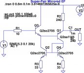
A small transformation to the previous schematic (swap T1 and T3, flip the current mirror and load) yields the following schematic.
THD20 is even lower, mainly because the rearrangement of the load resistor R2 allows the entire incremental current through R2 || RL to be be mirrored and corrected (unlike the previous circuit).
THD20 is even lower, mainly because the rearrangement of the load resistor R2 allows the entire incremental current through R2 || RL to be be mirrored and corrected (unlike the previous circuit).
Attachments

Last edited:
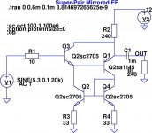
The previous circuit is already very good, but a further significant improvement is possible. Consider the collector current in the first (NPN) follower - it is very close to the emitter current in the output (PNP) follower. It can simply be diverted into the load as shown below; this halves the operating current of both followers. More importantly, it also removes the Vce variation on Ic (Early effect) from the first follower.
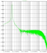
Net effect: H2 almost vanishes at around -130..140 dB, as shown below.
Further improvements are possible, for instance thorugh the use of a Wilson current-mirror in place of the stock 2-BJT current-mirror shown. However, it's likely that any further returns will be diminishing.
Net effect: H2 almost vanishes at around -130..140 dB, as shown below.
Further improvements are possible, for instance thorugh the use of a Wilson current-mirror in place of the stock 2-BJT current-mirror shown. However, it's likely that any further returns will be diminishing.
Attachments
Last edited:
What are the chances that a real world implementation will be -210dB down?
And, have you tried to look at the FFT of a two tone IM source and compare the the implementations - not sure that it works right in sims, but maybe it will show something of interest?
It looks too clean to be true, just guessing.
_-_-bear
And, have you tried to look at the FFT of a two tone IM source and compare the the implementations - not sure that it works right in sims, but maybe it will show something of interest?
It looks too clean to be true, just guessing.
_-_-bear

H2 is around -135 dB, not -210 dB. That's within reach of the top-end opamps today, even for large-signal unity-gain buffers, so I see no reason why a 4-BJT circuit can't achieve -135 dB for small signals (~100 mV amplitude). The Wilson Current Mirror reached close to this level (for currents, not voltages) about ~50 years ago, using only 3 BJTs.
IMD simulations on LTspice are possible, but will require a large number of cycles to complete - at least 380 cycles for a 19 kHz + 20 kHz transient response simulation. It can be done with a bit of patience - however, in this case it probably will not yield any significant insight above what is already available with a single sinusoidal transient response simulation.
If the transistors are from the same batch and hand-matched for beta fairly closely, a physical implementation of this circuit will yield results that are within +/- 20 dB of the simulated numbers. It's only a simple 2-stage voltage follower, nothing exotic or special.
Hi linuxguru,
That looks very interesting. Perhaps it would be a good buffer for between my CD player and power amplifier?
However I do not know too much about solid state (because I use tubes mostly!), so I would like to ask:
1.
How to bias the first transistor? (Is that a 5.3 V DC bias offset in the simulator?)
2.
As there are three NPN and one PNP transistors, might this lead to temperature related issues?
3.
How to calculate the output impedance of circuit 3?
4.
Which transistor types would be used for a 2V RMS signal, and what is the likely performance?
5.
Does the performance suffer when fed from a higher source impedance (say 2.5K to represent a 10K potentiometer at mid point)?
I feel as if I have asked too many questions?!?
1. How to bias the first transistor? (Is that a 5.3 V DC bias offset in the simulator?)
That was just a simulation schematic, mainly for the purpose of showing its design goals/principles in an uncluttered manner. It is a building block, much like the Wilson Current Mirror, and needs additional circuitry to make it useful. I have a Headphone Amp in the early stages of design, using this buffer as the output stage, which I'll post later.
To bias it, you can simply use a resistive divider between Vcc and Ground. A small input DC blocking capacitor to the base will complete the input side. That 5.3V is not important - I used it mainly to get 6V across R2 in the first schematic, which sets a bias current of 2.5 mA for all the transistors.
2. As there are three NPN and one PNP transistors, might this lead to temperature related issues?
Hmm - not unless they're mismatched, which of course can happen in the real world. In practice, one would mount Q1 and Q3 in close thermal contact, and similarly for Q2 and Q4.
3. How to calculate the output impedance of circuit 3?
It can be analysed with a bit of sweat and tears using the AC small-signal Hybrid parameters of the two transistors, but that's overkill here. You can get a first-order simulation approximation by grounding the input, injecting a small voltage signal at the output and measuring the current swing in LTSpice.
4. Which transistor types would be used for a 2V RMS signal, and what is the likely performance?
It depends on what kind of impedance you plan to drive. If it's high impedance (say more than 1k), just about any small-signal complementary BJT pair will work. My current favourites are the Toshiba 2sa970/2sc2240, but bc550c/bc560c or 2sa1015/2sc1815 should all work fine, with performance in the same ballpark as shown.
5. Does the performance suffer when fed from a higher source impedance (say 2.5K to represent a 10K potentiometer at mid point)?
Yes, it will. The most likely uses of this buffer will have an intervening op-amp on the input side for low-level signal handling and conditioning. The bigger problem is that there may well be instability when driven by a high-impedance source, which will have to be cured by appropriate compensation and degeneration (I omitted all those details in the simulation schematics, but they will be required in a real design).
Its a half diamond buffer...
But on the other hand, the emitter currents are held equal.
Thus one might hope the emitter voltage drops are equal.
And what comes out exactly the same as what goes in...
Yet buyer beware: one is NPN, the other PNP.
Are complimentary emitters ever really the same?
If the load misbehaves (like a loudspeaker for example)
Are the emitter currents still the same? Drawings 2 and
3 maybe, but probably not drawing #1...
Perhaps if you Wilson, then Q2 becomes the transistor
dumbed down to a diode. And then change it out for
a PNP??? Now mirror currents might not be equal, but
thats not the real question! Are emitter voltage drops
in Q1 and Q3 equal? Isn't that what matters most?
Or one could add a series diode (dumbed transistor) to
the emitters of Q1 and Q3, constructed of the opposing
PN type. That too would make drops equal, if currents
are equal.
Last edited:
J1 might ideally be selected for 0VGS at the quiescent current.
Your Q3 sees nearly the same voltage at collector as base, but
your Q1 operates with collector nearly at ground, so these two
aren't gonna be too similar in emitter voltage drops or thermals.
I hooked the collector of Q3 back to the top rail, just so its
dissipating more or less the same Wattage as Q1. A better
soloution might have been to cascode Q1, so that it also
sees only one emitter drop worth of collector voltage. But
I didn't think of that tweak in time, too lazy to redraw now.
Attachments
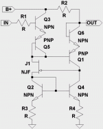
On further thought, ALL transistors in this circuit see the same current swing
as the output transistor. Thus, there is probably no suitable JFET that could
handle that demand for J1 in my drawing. Have to settle for another BJT here,
or go to the 4 transistor Wilson if we wanna obsess on collectors being equal.
as the output transistor. Thus, there is probably no suitable JFET that could
handle that demand for J1 in my drawing. Have to settle for another BJT here,
or go to the 4 transistor Wilson if we wanna obsess on collectors being equal.
Last edited:
Member
Joined 2009
Paid Member
StevenOH - Thanks for the patent references. The present schematic #2 is substantially similar to that in #4420725, except that Vout is located differently (albeit equivalently). The other two patents seem to be symmetric/push-pull elaborations of #4420725. Anyway, the good news is that all three patents have expired, and in any event, none of them covers schematic #3 (funky - I hit on #3 within 30 mins of getting #2).
If the good folks at Pioneer Japan hit on this idea in the late '70s, it can't be a bad idea - definitely worth investigating further.
If the good folks at Pioneer Japan hit on this idea in the late '70s, it can't be a bad idea - definitely worth investigating further.
Your circuits represent good thinking. The improvement of circuit#3 exploits the effect described in Hawksford's Slope Distortion Reduction article from 1988:
http://www.essex.ac.uk/csee/research/audio_lab/malcolmspubdocs/J10 Enhanced cascode.pdf
And it is good to know, that the ideas you came up with are validated by someone else.
(And Pioneer did use their circuits in several expensive and Japan-only amps.)
http://www.essex.ac.uk/csee/research/audio_lab/malcolmspubdocs/J10 Enhanced cascode.pdf
And it is good to know, that the ideas you came up with are validated by someone else.
(And Pioneer did use their circuits in several expensive and Japan-only amps.)
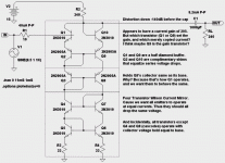
Wow - that's an imposing ladder. I'll try to get my mind around it - however, at first glace it seems that Q3-Q8 are overkill/unnecessary. Anyway, let me see how it sims in LTSpice.
Current gain is limited to ~beta of Q1, so 205 looks about right. It pays to have a high-beta BJT there, but the flip side of that is it may be hard to find a matching PNP Q9 with similar beta.
Current gain is limited to ~beta of Q1, so 205 looks about right. It pays to have a high-beta BJT there, but the flip side of that is it may be hard to find a matching PNP Q9 with similar beta.
- Status
- This old topic is closed. If you want to reopen this topic, contact a moderator using the "Report Post" button.
- Home
- Amplifiers
- Solid State
- Low-distortion Super-pair Buffer simulation schematics