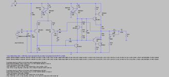
This is a design I will be trying to build in real life, but the problem is that I am getting oscillations in my output signal, when the input signal is around 2kHz or below, I do not have these oscillations, but greater, I would have them. Any idea? I also set upped the same circuit in Multisim 14.3 but I do not have these oscillations, it can handle even 20kHz input and output same 20kHz amplified.

Attachments
I managed to solve it. Turns out, I just needed an emitter degeneration on Q3. I consulted a book by Bob Cordell on designing power amps, it says that a 10:1 degeneracy resistor should help linearize the operation of the VAS stage.
Since mine is operating in ~6mA, the dynamic emitter resistance is computed as 26mV/6mA =4.33ohms. A 10:1 degeneracy resistor just literally means I need to add a resistor on the emitter of that transistor with a value 10 times the dynamic emitter resistance, it is 43ohms, since there is no 43ohms in the market, I set it to 47ohms.
Adding 47ohms on the emitter, I was able to get clean sine wave output even at 20kHz.
Attachments
A Bodeplot with ngspice shows the impact of the degradation resistor (red/blue w/o res, yellow/green with res):

I am not good with reading bode plots. But all I can see is that the dB seems linear even at high frequencies, it does eventually fall off but without the degeneration resistor, there seems to be a spike before it completely falls at high frequencies. When there is a degeneration resistor, no spike like the one without. So I guess it is good if there is a degeneration resistor.A Bodeplot with ngspice shows the impact of the degradation resistor (red/blue w/o res, yellow/green with res):
View attachment 1162719
It is indeed large, but it is the only cap value I found while experimenting that won't give me oscillations at the output.the 470p pole splitting cap C4 value seems excessively large
This one in particular is the output (in is 0.77V at 20kHz), when the pole splitting cap value is at 470pF:
While this one is when it is at 100pF:
47pF:
Is there a difference in the models between LTspice and Multisim?
Have you looked at the step response of the circuit? Or performed a stability analysis? The approach I use here (Taming the LM3886 - Stability) is pretty good as long as you insert the LC used for the test at a spot that has a low drive impedance and high load impedance.
Tom
Have you looked at the step response of the circuit? Or performed a stability analysis? The approach I use here (Taming the LM3886 - Stability) is pretty good as long as you insert the LC used for the test at a spot that has a low drive impedance and high load impedance.
Tom
1. Q9 and Q12 need either CE caps or base resistors. This current source can work without them if the transistors are different, i.e. one is faster.
2. And a CFP output should have a Zobel network.
3. Degenerating Q1 and Q2 is a better idea than Q3.
4. More than 150p C4 should not be needed, means there is another problem.
2. And a CFP output should have a Zobel network.
3. Degenerating Q1 and Q2 is a better idea than Q3.
4. More than 150p C4 should not be needed, means there is another problem.
My suggestion:
1. The transistors 2SC1815 and 2SA1015 are a bit slow for the front end and not large enough for drivers, but I kept them anyway.
2. You need to keep the HF base impedance of the LTP low to get as much speed as possible. An input cap is both a HF filter and low-Z to the base for feedback stability. The feedback divider is ~ok at 2.2K but more is a problem.
3. A "speed-up" cap across the driver bases deals with the asymmetric stability.
4. LTP degeneration is required for stability with a rational C comp, and much better for slew/ TIM.
5. The HF output loading is critical for CFP outputs, so I have added the standard Zobel and build-out network.
I would change more but these are the most important.
Attachments
Just curious what is the Current of Q4 / Q5
with resistors R13/R12 at 47 ohms?
Current would be cooking around 40 to 50 mA
To-126 package driving a CFP doesnt need more than
5 to 6 mA assume R13/R12 would be way closer to
220 ohms.
Anyways if using tip 2955 and 3055
transition frequency is not much more than .5 to 2 Mhz
with CFP cross conduction would start pretty early.
usually the negative rail rings. seeing the positive rail ringing
in the early examples. tells me there is just basic problems
with the circuit. Once correct
getting the output to not ring is more easily compensated
in the feedback loop or differential input.

For simulation sake
The half supply reference at the input R2 / R3
could not just be 2 resistors on the input in real life.
R2 would need gracious amounts of decoupling
to work.
could be likely why one sim didn't oscillate
and one did.
This is single supply amplifier, which needs DC offset
set on the outputs correctly.
The fact the positive rail is ringing not the negative.
Just drives me even further to think. DC offset
is way positive and no half supply decoupling.
the amplifier would ring like crazy.
Major clue is R5 at 270 ohms?
That would be way up to 560 or 680 ohms.
The differential input current and the half supply reference
are way out of balance.
Current sources are set to around 4mA
Diff input only needs 2mA
Vas or second gain stage needs closer to 6 to 8mA
7mA acceptable so the VBE or bias wont be jumpy for
CFP
I guess the blocking cap can be at the end
But makes more sense to block DC first on output.
then add the corrective networks.
I assumed the drivers were very high.
But they are still at 10mA which would cook them
and since bias is mainly determined by the drivers.
10mA would heat them up and likely cause thermal issues.
Drivers dont need more than 4 to 5mA
Yes, the input should be decoupled/filtered. I show the driver current as about 12mA in simulation (and 0.65/47=13.8mA), but 100 Ohms on the OP base is marginal for shoot through and turn-off time, 80% of BJT amp failures. You can cross-couple a CFP with a small cap(+R), but a larger cap creates PSRR problems. Yes, the IPS current is high but I left it as is. The VAS base resistor should be 2x+ the ccs resistor, but a current mirror would be better. Again, minimal changes. 1K on the feedback divider is better than 2k5 but there is no reason to do the same to the positive input. ~Zero at high frequencies is the ideal, but you can't do that on the negative input. I have used a RC+RC network for 50 Ohms @ ~100MHz. You want all other poles besides the (VAS) dominant pole to be as high as possible. Yes, the drivers seriously need to be bigger, 1 Amp or larger and 5 or 10 Watts. I would put the output cap after the Zobel network, in case the 2200uF cap has high ESR and/or inductance. Single supply amps have to be wired carefully to avoid sharing "ground" with the OP supply. There is a better way to do single supplies, ie an amp derived floating ground.
- Home
- Design & Build
- Software Tools
- LTSpice Getting Oscillations in Output but none in Multisim

