Hello people ! I need a help to modify the attachment switching circuit voltages in 3 stages for power amplifier Class H tensions rise and decem linearly according to the power demand required at the output stage
This circuit works with mosfets channel and N-channel-P ... would like to replace the P-channel fets for it to work only with channel-N ... if someone can me
help with some tips I'm very grateful ...
*
Best regards,
*
ernovbr
This circuit works with mosfets channel and N-channel-P ... would like to replace the P-channel fets for it to work only with channel-N ... if someone can me
help with some tips I'm very grateful ...
*
Best regards,
*
ernovbr
Attachments
Anyone have a suggestion for my problem ... someone with knowledge of mosfet please help me !!
ernovbr
ernovbr
Tank you
Friend andrew lebon this circuit the voltage variables are linearly or step?
Best regards,
Ernovbr
Friend andrew lebon this circuit the voltage variables are linearly or step?
Best regards,
Ernovbr
Hi Guys
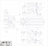
If you look at the Apex circuit, you see that between the voltage look-ahead references and the mosfets is a level shift circuit on the negative side - the rest is essentially the same. The IR2116 is a mosfet driver that allows up to 600V difference between the control side and the gate driver. The input is a Schmitt gate with well-defined transition for high and low output. Some manufacturers use a comparator here.
Most circuits of this type are supposed to switch hard to reduce mosfet power dissipation. However, they usually switch a bit softer than that and there is a small compromise of heat. There is also a slight lag on the way down voltage-wise. Using mosfets with the lowest Rds-on allows the best switching and symmetric clipping overall.
The abrupt supply current changes need to be isolated through physical ground routing and proper filtering. Sims and real life show the glitching on the feedback signal even if the output is clean. Most commercial amps of this type have adequate but not ample filtering based on expected music time cycles of power required at each supply level. Building your own, you should allow another rack space to have better heat sinking and more room for filtering.
Have fun
Hello friend, I modified the circuit switcher to work in series ... this worked well .... except that the resistors {negative side R37- R38 - R53 - R54 and positive side R31- R32 - R45 - R46} are heating up above normal,smoke comes out ...
Even with speakers when required resistor out a strong smell of burning.
See if you can give me a help there to solve this problem ...
Best regards,
ernovbr
Even with speakers when required resistor out a strong smell of burning.
See if you can give me a help there to solve this problem ...
Best regards,
ernovbr
Attachments
Last edited:
Hi Guys
The 8R2 base resistors for the level shift BJTs seems low. Since there is current gain in the level shift circuit, these Rs can be a bit higher. Typically you see 10k or higher on the higher rails, which still seems low.
It is more usual to have a voltage look-ahead circuit to feed the detectors. The look-ahead is just a cap with zener across it, charged up through the resistors tied to the detection cricuits. For example, R14, D8 and E3 in Apex's circuit above for the high-positive rail. The cap always has 18V across it set by the zener, and this rises above the rail ahead of the signal approaching the rail. This in turn lets the detector circuit turn on the mosfet. In the simplest circuits, the detector and the mosfet are the same but you have to use complementary mosfets for split rails.
I thought you wanted to use n-channels on both sides? To do that you simply add a level shift circuit on the negative side - this what the two BJTs do.
Have fun
Hi Guys
The 8R2 base resistors for the level shift BJTs seems low. Since there is current gain in the level shift circuit, these Rs can be a bit higher. Typically you see 10k or higher on the higher rails, which still seems low.
It is more usual to have a voltage look-ahead circuit to feed the detectors. The look-ahead is just a cap with zener across it, charged up through the resistors tied to the detection cricuits. For example, R14, D8 and E3 in Apex's circuit above for the high-positive rail. The cap always has 18V across it set by the zener, and this rises above the rail ahead of the signal approaching the rail. This in turn lets the detector circuit turn on the mosfet. In the simplest circuits, the detector and the mosfet are the same but you have to use complementary mosfets for split rails.
I thought you wanted to use n-channels on both sides? To do that you simply add a level shift circuit on the negative side - this what the two BJTs do.
Have fun
Sorry, not 8R2 correct value 8K2-5W ... about using only N-channel, I yes ... if possible send me the circuit to do this
Hi Guys
ernovbr - I don't see how your circuit works? It looks like the sexes of the BJTs are reversed, but... you say it works...
Anyway, attached is a drawing of the standard complementary mosfet switching method used by many amp companies. Since you already have complementary mosfets, it is worth a try since it is dead simple. Note that each mosfet is driven by its own gate circuit tied to the look-ahead voltage reference, so each gets a 10k-2W, a 100R gate-stop and the speed-up diode.
There is also a drawing for replacing the P-channels on the negative side with N-channels. A small P-channel is used as the interface so the voltage look-ahead works the same way. R10 and R12 should be 10k each NOT 100 as shown.
Have fun
Attachments
Last edited:
- Home
- Amplifiers
- Solid State
- Mosfet switching steps 3 p / class H amplifier