March 2025 marks the 20th anniversary of Mauro Penasa's "modest contribution to this forum" (his own words) - the "MyRef" composite LM3886 amplifier. I thought the anniversary is a good excuse to design a new board for the MyRef. It turned out pretty nice, so I'm sharing the results.
The MyRef remains one of the few published composite chipamp designs. I built my first MyRef back in 2011 - on Mauro's original board, with my own relay-based 96-step volume control - but I always wanted to build a better version.
Here it comes, mounted on a 2U (80mm) heatsink:

The board for one channel is 90x50mm, all through hole, with two layers. The schematic (see post #3 below) closely follows Mauro's original Rev.C. However, I took the liberty of adding regulators to the LM318's power supply; the two TO-220 regulators are visible in the photo above. The board includes neither raw power supply nor speaker DC protection, both of which I implemented separately.
The linearity is pretty nice for such a simple amplifier:

More spectra are attached to the post #14 below.
Also, while developing the above board, I designed another, for a simple non-inverting LM3886 based amplifier according to the datasheet schematic:

Mechanically, this board is identical to the other one. My objective was to test some ideas for board layout and routing, but this board also turned out quite nice in its own right. The schematic is attached to the post #15 below, measurements - to #16.
The MyRef remains one of the few published composite chipamp designs. I built my first MyRef back in 2011 - on Mauro's original board, with my own relay-based 96-step volume control - but I always wanted to build a better version.
Here it comes, mounted on a 2U (80mm) heatsink:
The board for one channel is 90x50mm, all through hole, with two layers. The schematic (see post #3 below) closely follows Mauro's original Rev.C. However, I took the liberty of adding regulators to the LM318's power supply; the two TO-220 regulators are visible in the photo above. The board includes neither raw power supply nor speaker DC protection, both of which I implemented separately.
The linearity is pretty nice for such a simple amplifier:
More spectra are attached to the post #14 below.
Also, while developing the above board, I designed another, for a simple non-inverting LM3886 based amplifier according to the datasheet schematic:
Mechanically, this board is identical to the other one. My objective was to test some ideas for board layout and routing, but this board also turned out quite nice in its own right. The schematic is attached to the post #15 below, measurements - to #16.
Last edited:

I built a few versions of Maura Penasa RIP MyRef amps and I would also build your version.
Looks like the Cin is missing and the Rground is gone too.
Great amp, waiting for more measurements.
Looks like the Cin is missing and the Rground is gone too.
Great amp, waiting for more measurements.
Indeed, Cin is omitted, but Rground (a.k.a. Ground Loop Breaking Resistor) is there as R4:

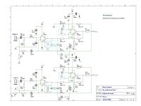
The MyRef's design - the original Rev.C schematic is attached below for easy reference - is covered in Mauro's detailed design note, a copy of which, machine-translated to English, is also attached. The schematic has also been looked at in both Mauro's original thread and ClaveFremen's thread on the Fremen Edition with ~5k posts each. In case of TL;DR and at the risk of beating a dead horse, here is a quick recap of the remaining parts.
The MyRef is a composite amplifier, with two opamps work together inside a common feedback loop. The first opamp (U1 in the schematic above) drives the other (U2), which is configured, with resistors R7 R8 R10 R11 R14, as a voltage controlled current source known as the Howland current pump. The transconductance of the pump is about 1A/V with the values shown - that is, one volt at U1's output translates into one amp of U2's output current. The output voltage is fed back to U1 via the divider R2 R13, which sets the gain of the amplifier relatively high, at 12k/390+1=31.77 V/V = 30dB. C1 drops that gain to unity at DC so that U1's DC offset voltage is not amplified by 30dB. R3 C2 form an input low pass filter, protecting the input of U1 from overload with RF and fast transients. The corner frequency of the filter is 220kHz nominally, but can be lower as the output impedance of the signal source combines with R3. For example, if the input is connected to a 50k volume control pot set to -6dB, the corner frequency becomes 45kHz. R1 provides a path to the ground for the input current of U1. The remaining parts are for frequency compensation - I'll comment on that separately.
The board also includes a regulated power supply for U1 and a bank of capacitors for U2:

Nothing unusual there. Two points maybe worth mentioning are the passive RC filters in front of the regulators (which filters also drop about 5 volts each to make the regulator's job easier) and powering the MUTE pin of the LM3886 from the regulated negative rail, so that U2 does not un-mute before U1 is ready.
The MyRef's design - the original Rev.C schematic is attached below for easy reference - is covered in Mauro's detailed design note, a copy of which, machine-translated to English, is also attached. The schematic has also been looked at in both Mauro's original thread and ClaveFremen's thread on the Fremen Edition with ~5k posts each. In case of TL;DR and at the risk of beating a dead horse, here is a quick recap of the remaining parts.
The MyRef is a composite amplifier, with two opamps work together inside a common feedback loop. The first opamp (U1 in the schematic above) drives the other (U2), which is configured, with resistors R7 R8 R10 R11 R14, as a voltage controlled current source known as the Howland current pump. The transconductance of the pump is about 1A/V with the values shown - that is, one volt at U1's output translates into one amp of U2's output current. The output voltage is fed back to U1 via the divider R2 R13, which sets the gain of the amplifier relatively high, at 12k/390+1=31.77 V/V = 30dB. C1 drops that gain to unity at DC so that U1's DC offset voltage is not amplified by 30dB. R3 C2 form an input low pass filter, protecting the input of U1 from overload with RF and fast transients. The corner frequency of the filter is 220kHz nominally, but can be lower as the output impedance of the signal source combines with R3. For example, if the input is connected to a 50k volume control pot set to -6dB, the corner frequency becomes 45kHz. R1 provides a path to the ground for the input current of U1. The remaining parts are for frequency compensation - I'll comment on that separately.
The board also includes a regulated power supply for U1 and a bank of capacitors for U2:
Nothing unusual there. Two points maybe worth mentioning are the passive RC filters in front of the regulators (which filters also drop about 5 volts each to make the regulator's job easier) and powering the MUTE pin of the LM3886 from the regulated negative rail, so that U2 does not un-mute before U1 is ready.
Attachments
Looks like the design note attached above was not fully translated. I apologize and re-attach the same note, now fully translated. Translation is not perfect but clear enough IMO.
The board for one channel is 90x50mm, all through hole, with two layers:

Unlike most chipamp boards and much like the PCBs that follow the diyAudio Universal Mounting Specification, it mounts parallel to the heatsink on 6mm standoffs. The mounting pattern is sort of UMS compatible, with four holes in the corners of a 80x40mm rectangle and an additional one in the center for the LM3886's mounting screw. The LM3886 mounts on the heatsink under the board, parallel to it:

It takes a little lead bending but works very well, eliminating mechanical issues like obstructed access to LM3886's mounting screw, while helping to improve layout:

The board for one channel is 90x50mm, all through hole, with two layers:
Unlike most chipamp boards and much like the PCBs that follow the diyAudio Universal Mounting Specification, it mounts parallel to the heatsink on 6mm standoffs. The mounting pattern is sort of UMS compatible, with four holes in the corners of a 80x40mm rectangle and an additional one in the center for the LM3886's mounting screw. The LM3886 mounts on the heatsink under the board, parallel to it:
It takes a little lead bending but works very well, eliminating mechanical issues like obstructed access to LM3886's mounting screw, while helping to improve layout:
Attachments
Last edited:
Nice work here Alexcp!
I especially like the undermounting of the LM3886 chip, that opens up better chassis options for sure. Never liked the perpendicular “stand up” mounting method. 👍🏻
I especially like the undermounting of the LM3886 chip, that opens up better chassis options for sure. Never liked the perpendicular “stand up” mounting method. 👍🏻
Nice work here Alexcp!
I especially like the undermounting of the LM3886 chip, that opens up better chassis options for sure. Never liked the perpendicular “stand up” mounting method. 👍🏻
Yes, nice thinking outside the box. Would there be any issue with heat transfer back into the PCB with this orientation?
Nope, the LM3886 is not touching the pcb, it's mounted to the HS. I'd guess the pcb would get no hotter than the chassis interior ambient temperature which would never be an issue for this type of amplifier.
Just think how hot the pcb gets in a Class A amplifier.

Just think how hot the pcb gets in a Class A amplifier.
No, PCB heating by the LM3886 is not a problem.
Here is my test build:

The chassis is a 330mm wide Mini Dissipante 2U 250mm from Modushop (internally, it is 250×250×80mm). Its front and back panels are temporarily replaced with some 1/4 inch (6 mm) MDF. The two amplifier boards are sitting on the heatsinks left and right. The two transformers (it's a dual mono) in the front are 100VA Anteks. Their primaries are not properly wired; I just crimped FASTON terminals to connect them for tests. In the middle, there are two raw power supply boards (I'll cover them later) and in the back, two DC protection boards that were designed for a different project and are being reused here.
The whole thing is quite cool unless it continuously delivers 70 W into 4 ohms.
Here is my test build:
The chassis is a 330mm wide Mini Dissipante 2U 250mm from Modushop (internally, it is 250×250×80mm). Its front and back panels are temporarily replaced with some 1/4 inch (6 mm) MDF. The two amplifier boards are sitting on the heatsinks left and right. The two transformers (it's a dual mono) in the front are 100VA Anteks. Their primaries are not properly wired; I just crimped FASTON terminals to connect them for tests. In the middle, there are two raw power supply boards (I'll cover them later) and in the back, two DC protection boards that were designed for a different project and are being reused here.
The whole thing is quite cool unless it continuously delivers 70 W into 4 ohms.
Last edited:
That is one well packed little chassis, looks great.
Any issue with the trafos so close to the amp boards?
Any issue with the trafos so close to the amp boards?
Here is the above setup with Antek 1222 (2×22VAC rectified to approx. +/-28VDC) driving 30W into a 8ohm load at 1kHz:

There is a bit of hum at -120dB (that’s 15 μV) which I will show later is not present when the board is powered by a lab power supply. I have not investigated the exact source of this hum - most likely it is inductive coupling into signal wiring, but it can also be the board's PSRR or even my measurement setup's fault. At this point, I don't think it's a huge problem.
There is a bit of hum at -120dB (that’s 15 μV) which I will show later is not present when the board is powered by a lab power supply. I have not investigated the exact source of this hum - most likely it is inductive coupling into signal wiring, but it can also be the board's PSRR or even my measurement setup's fault. At this point, I don't think it's a huge problem.
Last edited:
The rectifier is more likely to couple into sensitive circuits than the transformer itself. That said, there's a lot of excess wiring that could be trimmed off.
-120 dBc hum is not a big deal, though it'll wreck the THD+N as it becomes part of the +N. That's a bit unfortunate. It'd be nice to know where it comes from.
Tom
-120 dBc hum is not a big deal, though it'll wreck the THD+N as it becomes part of the +N. That's a bit unfortunate. It'd be nice to know where it comes from.
Tom
I get that 15 μV hum peak on my QA403 even with all inputs shorted (!), running off a battery powered notebook, as long as the ground of QA403 (the outer shell of one of the BNC connectors) is connected to the amplifier's ground. I'll look into it further, but it is clear that the amplifier's boards is not the (only) source of that.
There is a school of thought that says that for better sonics, it is better to have approximately flat THD+N vs frequency. For a feedback amplifier, that would usually mean flat loop gain vs frequency in the audio band. Mauro's original Rev.C frequency compensation achieves exactly that. The LM318 is internally compensated for unity gain but allows adding external external frequency compensation as required. Mauro used this to create a flat 50dB loop gain in the audio band. Here is the simulated global (outer) loop gain (there are two additional local NFB loops, one around the output stage of the LM318, the other, around the LM3886):

(the LM318 model used for this simulation is courtesy of RCL-electro.ru).
However, because of this compensation, Mauro's Rev.C has not-quite-perfect clipping behavior:

Personally, I don't think this is a serios issue, yet I took the liberty to adjust the compesation a little to improve clipping behavior. I changed the values of the RC network between the inputs of the LM3886 from the original 1nF+3.3kOhm :

to 3.3nF+2kOhm:

This improves the clipping behavios somewhat:

without changing the loop gain in the audio band:

This change is optional but looks like a no regret move to me.
(the LM318 model used for this simulation is courtesy of RCL-electro.ru).
However, because of this compensation, Mauro's Rev.C has not-quite-perfect clipping behavior:
Personally, I don't think this is a serios issue, yet I took the liberty to adjust the compesation a little to improve clipping behavior. I changed the values of the RC network between the inputs of the LM3886 from the original 1nF+3.3kOhm :
to 3.3nF+2kOhm:
This improves the clipping behavios somewhat:
without changing the loop gain in the audio band:
This change is optional but looks like a no regret move to me.
Last edited:
Although my investigation of hum and noise is ongoing, here are some spectra showing THD and IMD performance. All measurements are taken with a regulated lab power supply set to +/-35V and a resistive load.
1kHz 1W into 8ohm:

1kHz 40W into 8ohm:

1kHz 67W into 4 ohm (note MyRef has only half the loop gain with a 4ohm load compared to that with a 8ohm load, so distortion has to be higher):

IMD 18+19kHz 1:1 "40W" (meaning the same 80W peak power as a 40W/8ohm sinewave) into 8ohm:

IMD 60Hz+7kHz 4:1 "40W" into 8ohm:

IMD 1+5.5kHz 1:1 "40W" into 8ohm:

1kHz 1W into 8ohm:
1kHz 40W into 8ohm:
1kHz 67W into 4 ohm (note MyRef has only half the loop gain with a 4ohm load compared to that with a 8ohm load, so distortion has to be higher):
IMD 18+19kHz 1:1 "40W" (meaning the same 80W peak power as a 40W/8ohm sinewave) into 8ohm:
IMD 60Hz+7kHz 4:1 "40W" into 8ohm:
IMD 1+5.5kHz 1:1 "40W" into 8ohm:
Last edited:
The other amplifier board is a simple non-inverting LM3886 as per the datasheet:

The 90x50mm, all through hole, two layer board is mechanically identical to the MyRef board above. Here both of them are side by side for comparison, with MyRef on top:

The layout is similar but obviously simpler:

The board works with no surprises. Here is 1kHz clip into 8 0hm with +/-35V supplies:

and the same into 4 ohm with +/-28V supplies:

Distortion spectra will follow.
The 90x50mm, all through hole, two layer board is mechanically identical to the MyRef board above. Here both of them are side by side for comparison, with MyRef on top:
The layout is similar but obviously simpler:
The board works with no surprises. Here is 1kHz clip into 8 0hm with +/-35V supplies:
and the same into 4 ohm with +/-28V supplies:
Distortion spectra will follow.
Last edited:
Here are the distortion spectra for the simple non-inverting LM3886. Again, resistive load, +/-35V regulated power supply for 8 ohm measurements, +/-28V for the 4 ohm THD. Not as low as the MyRef above, but pretty decent for a naked LM3886, and an improvement over e.g. my own 2018 boards.
1kHz 1W into 8ohm (THD = 0.0011% = -99dB)

1kHz 45W into 8ohm (THD = 0.0008% = -102dB):

1kHz 70W into 4ohm (THD = 0.0019% = -94dB):

IMD 18+19kHz 1:1 "45W" (i.e. 90W peak) into 8 ohm:

1kHz 1W into 8ohm (THD = 0.0011% = -99dB)
1kHz 45W into 8ohm (THD = 0.0008% = -102dB):
1kHz 70W into 4ohm (THD = 0.0019% = -94dB):
IMD 18+19kHz 1:1 "45W" (i.e. 90W peak) into 8 ohm:
Yes. Nice work Alexcp
The last few lm3886 gainclones I have done have been undermounted in this way. As you say it does open some new layout possibilities.
It would be nice if TI made a version with the pins pre bent that way.
@xschop I have never had a problem with overheating when mounted this way as Alexcp mentions.
The last few lm3886 gainclones I have done have been undermounted in this way. As you say it does open some new layout possibilities.
It would be nice if TI made a version with the pins pre bent that way.
@xschop I have never had a problem with overheating when mounted this way as Alexcp mentions.
The raw power supply is almost conventional:

Apart from the mandatory bridge rectifier and bulk capacitors, it has fuses (transformers are expensive and should be protected), an RC snubber, a separate rectifier for a LED, and an 1-ohm resistor RG between the secondary's center tap and the ground.
That RG is not my original idea - I borrowed it from another chipamp build (here; note the linked site has a bad certificate, so your browser will complain) and wanted to see how it works. The effect of that resistor is that it reduces audio frequency current through the (nonlinear) rectifier, making for cleaner supply rails. The result is easily measurable (see the spectra under the spoiler below), but the importance of it remains to be heard.
The raw power supply is built on its own 70x80mm PCB:

The rectifier is heatsinked (I used these heatsinks in my LME49830 build and had an extra couple sitting around) with a view to power some of my more power hungry builds, but for a chipamp, the heatsink proved to be unnecessary.
Apart from the mandatory bridge rectifier and bulk capacitors, it has fuses (transformers are expensive and should be protected), an RC snubber, a separate rectifier for a LED, and an 1-ohm resistor RG between the secondary's center tap and the ground.
That RG is not my original idea - I borrowed it from another chipamp build (here; note the linked site has a bad certificate, so your browser will complain) and wanted to see how it works. The effect of that resistor is that it reduces audio frequency current through the (nonlinear) rectifier, making for cleaner supply rails. The result is easily measurable (see the spectra under the spoiler below), but the importance of it remains to be heard.
The voltage of the supply rail is a sum of DC and AC component. The AC component is, in turn, a sum of a sawtooth wave with twice the mains frequency, a rectified version of the amplifier's output, and their intermodulation products. Here is the spectrum of the AC component on the power supply rail of the amplifier delivering a 1kHz sinewave into the load:

If we zoom in around, say, 1kHz, the intermodulation products at 1kHz +/-120Hz, +/-240Hz, etc. become visible:

The RG cleans up this spectrum a bit:

However, the spectrum is still dominated by the 120Hz sawtooth and the rectified 1kHz sine, and the addition of the RG does not change the output spectrum of the amplifier. I'll try to find out whether RG makes any difference sonically, but I am skeptical.
If we zoom in around, say, 1kHz, the intermodulation products at 1kHz +/-120Hz, +/-240Hz, etc. become visible:
The RG cleans up this spectrum a bit:
However, the spectrum is still dominated by the 120Hz sawtooth and the rectified 1kHz sine, and the addition of the RG does not change the output spectrum of the amplifier. I'll try to find out whether RG makes any difference sonically, but I am skeptical.
The raw power supply is built on its own 70x80mm PCB:
The rectifier is heatsinked (I used these heatsinks in my LME49830 build and had an extra couple sitting around) with a view to power some of my more power hungry builds, but for a chipamp, the heatsink proved to be unnecessary.
Last edited:
Unfortunately, I have not read all 10k+ posts either, so I have no idea what the consensus is. Personally, I built one Rev.C on Mauro's original single sided board and one Rev.C on my own board, pictured above. The latter is much better on measurement and sounds quite nice on the bench, but still awaits a critical listening session.
- Home
- Amplifiers
- Chip Amps
- MyRef 20th Anniversary Edition and a simple Reference LM3886 board