Hello All,
I looked over the first few pages of a diyAudio search for “KiCad”, and did not find anything that helps with my problems.
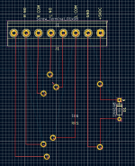
I am using V7 for this project. I have a very simple PCB design, nothing more than a terminal strip and pads to accept the relay pins. The reed relay is quite old (1980’s P&B T10 series, long out of production), but high quality, so I wanted to use them in this preamp project. I was unable to find a datasheet that provided pinout dimensions, so I had to design my own KiCad Footprint. Attachment 1 shows the board (the grid is 0.1270 mm). Running DRC results in many errors. Attachment 2 and 3 shows the two types of errors. I have spent almost a week trying to understand what is going on, but with no luck. What is strange, is that a week before I began this design, I did a separate board for mounting the switches that control these relays, that went without a hitch. So, I assuming it all revolves around my Footprint design, but that is just a guess.
Any help would be greatly appreciated.
Cheers,
ceulrich
I looked over the first few pages of a diyAudio search for “KiCad”, and did not find anything that helps with my problems.
I am using V7 for this project. I have a very simple PCB design, nothing more than a terminal strip and pads to accept the relay pins. The reed relay is quite old (1980’s P&B T10 series, long out of production), but high quality, so I wanted to use them in this preamp project. I was unable to find a datasheet that provided pinout dimensions, so I had to design my own KiCad Footprint. Attachment 1 shows the board (the grid is 0.1270 mm). Running DRC results in many errors. Attachment 2 and 3 shows the two types of errors. I have spent almost a week trying to understand what is going on, but with no luck. What is strange, is that a week before I began this design, I did a separate board for mounting the switches that control these relays, that went without a hitch. So, I assuming it all revolves around my Footprint design, but that is just a guess.
Any help would be greatly appreciated.
Cheers,
ceulrich
Attachments


I'd try specifying the top and bottom solder masks in the layer stackup. Pick a colour and go with the default settings to start.
Tom
Tom

Mark, thanks for the guidance. I checked all eight pads for the Footprint using the Footprint Editor and all had those two boxes checked.
Tom, not sure how to pick a color, I am at about a level two in understanding KiCad.
Tom, not sure how to pick a color, I am at about a level two in understanding KiCad.
Tom, sorry to be so dense, I now see how to set color for the F and B Mask. I did that, using purple (the OSH Park color), unfortunately no change in errors.
Hmmm... Silly question: Are the connections drawn on a copper layer? You'll want B.Cu for that. Or F.Cu if you'd rather have the traces on the top.
I'd set the minimum solder mask web width to something other than zero. I forget what OSH Park needs. 0.1 mm or so should be OK. The exact spec should be on their website.
Also draw a board outline. I forget if KiCAD requires one but I have had other tools barf if the outline was missing. You need to use the Edge.Cuts layer for this. I make the outline 50 mil wide so I don't get tempted to place the components too close to the edge of the board.
One way to shed light on this could be to un-select all layers in the viewer and then turn on the ones that you use one-by-one. I'd make sure that the copper layer looks correct and also that the solder mask looks correct. You should have features drawn where you need openings in the solder mask.
You could also try to upload the file to OSH Park or export to Gerber and look at the output with a Gerber viewer. Unless KiCAD is fundamentally broken (which I highly doubt) you're dealing with something super obvious.
Did you start with a schematic or did you create the netlist manually? I'm guessing the former.
Sorry to not be able to provide better help. I've only laid out a couple of boards in KiCAD (5.99 and 6.0) and I haven't come across this particular error.
Tom
Last edited:
Tom, thanks for the additional thoughts.
Yes, I did put the tracks on the F Cu layer.
I checked the OSH Park website, and found the minimum setting should be 4 mils (0.1mm) as you suggested. I made the change in Board Setup. No change to the list of errors.
I did start with a schematic. The global symbol library that loads with KiCad does not have a symbol for mechanical relays, so I made my own, and that may be where I went astray. In re-reading some KiCad docs, I find an example for making a relay symbol, and the process is nothing like I used. So, I will go back to square-one and see if I can duplicate that process.
Cheers,
ceulrich
You could also try creating a schematic with two footprints provided with KiCAD. That should not result in errors. Then add your own footprint.
Tom
Tom
Kicad considers your tracks as incorrect, I sometimes get this error if the track is associated with a net I changed the name of later. You can check like this:
Click on one track with the mouse, hit "i" on the keyboard to select the complete track, hit "e" to open the edit dialog and look at the net the track is associated to. You can change the net there. Normally Kicad does this automatically, but sometimes it gets stuck.
Another way is to simply delete a track and draw a new one: if the same happens it might be a problem with your symbol and/or footprint. The symbol in the schematic needs to have numbered pins so that the footprint "knows" which pin is connected where! If two pins have the same number Kicad wants you to connect them together, or it gets confused when 2 different nets are connected to 2 pins with the same number. Normally impossible, but if you change the footprint or symbol after drawing the layout it can happen.
So if you change something in the schematic or alter a footprint you need to update the footprints in the PCB and/or update the netlist from the schematic into the PCB - there are menu commands to do so.
Tom, yeah, my original idea was to use an existing DPDT switch symbol, and I added a rectangle with two pins to represent the coil, since I could not find an existing coil symbol. It seemed to work, but ….. I guess it didn’t.
My current approach is to scour the web for KiCad-compatible relay symbols, which I found, and downloaded. However, it seems they are in an older format that needs to be converted, and that took a number of hours to figure out. Then, of course there are the Library issues to figure out.
Hello jpk73, thanks for the suggestions. I tried the “i – e” sequence, but the dialog that opened does not have an option identified as a “net.” I get the same dialog if I select the track and open the “Properties” dialog. I have tried to work the different nets problem, but my reading suggests that Version 7 handles nets differently than previous versions. The only access to info on “Nets” is from the “Board Setup” menu, and is just about mechanical aspects of the different nets.
I can’t tell you how many times I have redrawn tracks. One of my first attempts, I kept getting the “track off grid” error, so I re-drew all tracks, that fixed the “off grid” problem, but I still had all the other errors.
As you suggest, the problem probably lies with pin identification, and that goes back to the way I created the original symbol and footprint. As mentioned above, I am going back to square-one and am going to try using an established relay symbol and making sure that my footprint is in sync.
This is a bit like a chimp sitting at a piano trying to play Mozart. Believe it or not, I have done successful boards (for an LM3886 amp) with Version 4.
Cheers,
I am on V5 and can assign the net for the selected track segments in a drop down menu. The FP can have pins that the symbol doesn't have, but the pins the symbol has should exist in the FP.
Replace the relay with a resistor. See if that works.
If you get the error when using two KiCAD provided symbols and footprints I'd ask in the KiCAD forum.
Tom
If you get the error when using two KiCAD provided symbols and footprints I'd ask in the KiCAD forum.
Tom
Jpk73, I have yet to find a way to determine or set a net for individual tracks in V7. For individual pads it is easy, just Select, open Properties, and there is a box for setting a net. If I set all pads for all components to “No Net”, the “Missing connection between items” errors are resolved. The pin count for all my symbols and footprints are consistent.
Nigelwright7557 and Tom; yeah, I am coming around to that idea. I have been reading a lot from that Forum as I search for answers. I thought I would read a bit more, to understand the Forum’s culture, so my question(s) would be properly directed.
Just an update, I redid everything using KiCad supplied relay symbols and footprints, and I am left with only one set of errors “Front solder mask aperture bridges items with different nets.” Off to the Forum!
Cheers,
ceulrich
Oh, joy. Best of luck. Please let us know what you find.Just an update, I redid everything using KiCad supplied relay symbols and footprints, and I am left with only one set of errors “Front solder mask aperture bridges items with different nets.” Off to the Forum!
Tom
Hello All,
Tom was spot on with his comment “you’re dealing with something super obvious.” It turns out I have been trying to draw tracks with the line drawing tool and not the Route Tracks tool. SLAP FOREHEAD WITH PALM OF HAND!!
Cheers,
ceulrich
Tom was spot on with his comment “you’re dealing with something super obvious.” It turns out I have been trying to draw tracks with the line drawing tool and not the Route Tracks tool. SLAP FOREHEAD WITH PALM OF HAND!!
Cheers,
ceulrich
For the curious, the solder mask layer is a "negative": it shows where you don't want a solder mask to be applied. The solder mask keeps solder from sticking to the underlying copper (or even substrate).
Normally you have a hole (called an "aperture" in PCB-land) in the solder mask over a pad so that the copper is exposed and solder sticks. However, if you have two pads close together, and the aperture covers both of them, then a glob of solder can stick to both, connecting them. So if they represent two different nets then KiCad complains. (This is the "solder mask aperture bridges items with different nets" error.)
Note also that if you don't want to see these errors (or any other DRC errors), you can turn them off in Board Setup > Design Rules > Violation Severity.
- Home
- Design & Build
- Software Tools
- Need Help With KiCad