Hi all, I've been working on a new DAC board, not because I am unhappy with the PCM1793 application I recently designed but rather because I suspect that correctly grounding 4 DACs sharing an I2S source will not be trivial.
This design employs two PCM4104 DAC ICs to handle up to 8 channels. These are 4-channel DACs, designed for high end/pro applications and feature a 118dB SNR spec:
Audio Converter - Audio DAC - PCM4104 - TI.com
However the reference design is on a fairly large 4-layer PCB. The challenge here was to get a suitable design within the Eagle lite limitation of 2-layers, 100x80mm. Hopefully I've managed it, though I don't expect to fully achieve the potential spec it should come close.
The output filters do away with the suggested 100uF coupling capacitors and I assume the result is that there may be a few mV offset present at the output, for me this is fine since the subsequent stage (volume controller) would be AC coupled. The filters were modelled in LTSpice to produce a result which can employ the most common component values:

About -6dB gain response by 100kHz, 4.2V RMS output level within pass-band for 0dBfs input (~ideal for driving my CS3318 for optimum SNR). Op-amp is OPA2227, slightly worse noise figure in this application than a BJT input one but very marginally so, SOIC-8 package keeps de-coupling capacitors very close.
No doubt there will be complaints about the old-tech LM317/337 pair 😱 , but with the C67/C70 22uF capacitors they are very low idle noise. They have relatively slow compensation circuits, but then they are powering an analogue audio stage with substantial bypass capacitance. Thermal dissipation should be comfortable, around 50C max assuming 25C ambient, the copper area may help a bit too.
Analogue 5V is by the LT1763 low-noise regulator and digital 3.3V by ADP3301, which is a regulator happy to be bypassed by large MLCC caps, so ideal for applications with switching transients. 5V reference comes by ADR02 reference which is hopefully more unconditionally stable the the analogue 5V rail; yes, the Vref pins are daisy chained however I assume virtually no current draw from any of them so this shouldn't be an issue.
The bottom copper is reasonably unbroken and is primarily treated as a ground plane. Analogue bypass capacitors for the PCM4104 are placed here on the underside, since there are many capacitors we want near to the IC it makes sense to use both sides of the board around them, the reference design does so.
Configuration is for 24-bit I2S data, no de-emphasis. Reset can be applied by grounding the reset pin. Single, double or quad rate can be selected by 2mm jumpers, or if these need to be regularly re-configured I suppose I can just connect them to the microcontroller. I've not seen a DAC which can't automatically adjust to the full range of sample rates before, unless there's a subtlety here?
The vias in the LRCK and BCK lines of the right hand DAC are unfortunate but I can't see a way round this. As recommended by Maxim, two vias are used in series to lower inductance, also these are relatively lower speed clock lines. Top copper pour is intentionally excluded from this I2S input area since nearby ground areas influence the characteristic impedance of these lines.
Any critique or questions welcome!
This design employs two PCM4104 DAC ICs to handle up to 8 channels. These are 4-channel DACs, designed for high end/pro applications and feature a 118dB SNR spec:
Audio Converter - Audio DAC - PCM4104 - TI.com
However the reference design is on a fairly large 4-layer PCB. The challenge here was to get a suitable design within the Eagle lite limitation of 2-layers, 100x80mm. Hopefully I've managed it, though I don't expect to fully achieve the potential spec it should come close.
The output filters do away with the suggested 100uF coupling capacitors and I assume the result is that there may be a few mV offset present at the output, for me this is fine since the subsequent stage (volume controller) would be AC coupled. The filters were modelled in LTSpice to produce a result which can employ the most common component values:
About -6dB gain response by 100kHz, 4.2V RMS output level within pass-band for 0dBfs input (~ideal for driving my CS3318 for optimum SNR). Op-amp is OPA2227, slightly worse noise figure in this application than a BJT input one but very marginally so, SOIC-8 package keeps de-coupling capacitors very close.
No doubt there will be complaints about the old-tech LM317/337 pair 😱 , but with the C67/C70 22uF capacitors they are very low idle noise. They have relatively slow compensation circuits, but then they are powering an analogue audio stage with substantial bypass capacitance. Thermal dissipation should be comfortable, around 50C max assuming 25C ambient, the copper area may help a bit too.
Analogue 5V is by the LT1763 low-noise regulator and digital 3.3V by ADP3301, which is a regulator happy to be bypassed by large MLCC caps, so ideal for applications with switching transients. 5V reference comes by ADR02 reference which is hopefully more unconditionally stable the the analogue 5V rail; yes, the Vref pins are daisy chained however I assume virtually no current draw from any of them so this shouldn't be an issue.
The bottom copper is reasonably unbroken and is primarily treated as a ground plane. Analogue bypass capacitors for the PCM4104 are placed here on the underside, since there are many capacitors we want near to the IC it makes sense to use both sides of the board around them, the reference design does so.
Configuration is for 24-bit I2S data, no de-emphasis. Reset can be applied by grounding the reset pin. Single, double or quad rate can be selected by 2mm jumpers, or if these need to be regularly re-configured I suppose I can just connect them to the microcontroller. I've not seen a DAC which can't automatically adjust to the full range of sample rates before, unless there's a subtlety here?
The vias in the LRCK and BCK lines of the right hand DAC are unfortunate but I can't see a way round this. As recommended by Maxim, two vias are used in series to lower inductance, also these are relatively lower speed clock lines. Top copper pour is intentionally excluded from this I2S input area since nearby ground areas influence the characteristic impedance of these lines.
Any critique or questions welcome!
Attachments


You can eliminate the thermal relief for the polygon that the LM317/337 use for their
heat sink...it will improve the heat sink effectiveness.
You can replace R62/R64 with a zener diode for much better ripple rejection.
If you do the zener trick, change R62/R63 = 121R.
Check here for more details on using the 317/337 this way.
The layout will take some time to analyze...looks pretty good on first glance.
I noticed another thing.
Some traces meet at a 45 degree angle.
Not considered good practice.
The traces under C24 are a good example.
The traces on the left are done wrong.
The traces on the right are done correctly.
Some traces meet at a 45 degree angle.
Not considered good practice.
The traces under C24 are a good example.
The traces on the left are done wrong.
The traces on the right are done correctly.
Sorry for late response, thanks for looking at this! I still hope to pursue this but have been much busier recently so not much happening right now. The LM317 article looks interesting, will give that a proper read through 🙂
Just another quick thought,
with regard to the ADR02 device, considering the increase in noise above 10Hz bandwidth would an RC post filter be wise? Some rough values might be 22R and 220uF.

I must assume input current to the Vref pins is both minimal and constant or this may do may harm than good, and I can only assume since the datasheet does not indicate!
I know that any noise on the the Vref pins will effectively pass straight through to the output and this is why I think it could be advantageous.
The LM317/337 are still under review but I do think they are quite capable and the choice of comparable devices is slim.
with regard to the ADR02 device, considering the increase in noise above 10Hz bandwidth would an RC post filter be wise? Some rough values might be 22R and 220uF.
I must assume input current to the Vref pins is both minimal and constant or this may do may harm than good, and I can only assume since the datasheet does not indicate!
I know that any noise on the the Vref pins will effectively pass straight through to the output and this is why I think it could be advantageous.
The LM317/337 are still under review but I do think they are quite capable and the choice of comparable devices is slim.
Been slow progress but here's a Rev 1!
This one is software controlled. I couldn't route the SPI to the right hand chip without cutting up the ground plane, so the intention is to use 3 short wires on the underside for this connection, it should be easy to route these neatly and they won't be visible. The SPI outputs aren't used, I don't imagine reading back the registers would ever be particularly useful, but the chips are individually addressable.
I added the reference voltage filter, can't hurt to add the pads I figure.
Fixed the 45 degree track meetings.
LM317/337 updated to use zener references. I tested this on breadboard; with the zener and rectifier diode bonded with sticky-tak the voltage remained completely stable over time. On the PCB a blob of resin or similar on these diodes may help keep thermal tracking. The regulators are now the TO-220 type, heat dissipation will be too high to use SMT parts now, a small heatsink isn't required but may be nice to use.
Thanks for looking and any input appreciated 🙂
Attachments


Looking good so far...
I found a few more 45 degree joints, near the following locations:
C3, C4, C71 and C88.
Try turning off thermals on your ground planes. It will make it slightly
harder to solder, but if you have a good iron, you wont even notice.
The thermals add unwanted inductance.
And for a cleaner finished look, go in design rules > mask > limit
and change the value to 24 mils. This will remove the mask from any
holes smaller than 24 mils (it will "tent" your vias). Pads are unaffected.
Glad to hear the regulator design worked as expected!
Oh, and if you are up for a challenge, standard naming convention starts
at the top, left and works its way to the bottom, right.
example: if you had half a dozen resistor scattered evenly across the board,
R1 would be the top, left; R2 would be bottom left; R3 would be top, center;
R4 would be bottom, center; R5 would be top, right; and R6 would be bottom,
right. This makes it easier to find components.
It looks like a nice layout however I haven't looked into it in any great detail.
Who cares about 45 degree joints! What you really need to take care of is all the TH components! If you have those DACs on there then I'm sure people can also solder 0805 or even 0603 - this will make the board so much more efficient and smaller.
Who cares about 45 degree joints! What you really need to take care of is all the TH components! If you have those DACs on there then I'm sure people can also solder 0805 or even 0603 - this will make the board so much more efficient and smaller.
For what purpose this board is designed, and in which system it will be used? For multi-way speakers? If yes then what kind of interface to DSP you've been considered? I ask this because I2S is not the only one possible with these converters, not not necessary the most practical one. Instead you might want to consider using TDM (DSP/I8S etc.) inteface, that would make the interconnects simpler - you need just one data line thats shared between two converters.
Also, it would be easier to put just a single PCM4104 on one board. That wouldn't add costs much (smaller boards are less expensive to buy). The on your DSP board you could have two similar headers. Then you just configure the other board to use TDM sub-frame 0 and the other sub-frame 1 (SUB pin connected either ot GND or to VCC).
Then it would be nice if there were some kind of standard layout for the headers so that you could easily use different DAC's. I am currently designing some test board for the LPC Link2 (JTAG debugger used as dev board) and I'm first building a header board to be used with the DACs I got from DIYINHK site. They have common layout, and I'm just adding an I2C port to that header layout. PCM4104 doesn't have I2C though but 4-wire SPI but it's not difficult to convert between them using some MSP430 controller (or the cheap LaundchPad kit). With LPCLink2 the SPI pins are shared with I2S0 which I need for input (the output is using SGPIO port), and I kind of wanted to keep it simple and not add too many pins. The DIYINHK (DIYINHK) layout is nice as it includes one extra GND pin so you can easily test you board using breadboard. Avoiding the vias will always be a challenge though.
Anyway you layout looks nice. It would be though nice it your work (if it will open source) would be useful to other folks. I think diyers should more consider that part and really start using some common header layouts and such. Even the power supplies could use standard headers (including sense signal pins someone would add propably) so you wouldn't have to always design one of your own (life is short).
Hi all, sorry been a busy week so not had much chance to revise the design.
I produced a new revision on Tuesday though which I'm attaching here. This design addresses a few issues.
Boscoe, the through hole parts are there for a few reasons. Chiefly, they allow me to route traces underneath, not many SMT parts are big enough for this. Additionally, they are common, cheap and can be matched quite easily with a multimeter. The breaks in the ground plane are unfortunate, minimelf is a possible alternative to avoid this but I found them really expensive to buy. The only resistor going to ground is right at the top anyhow so it gets a pretty clean connection to GND.
mhelin, lots to think about there. I hadn't considered anything other than I2S even though the IC does support it. I don't know how common any USB - I8S convertors are but the reduction in data lines would be nice.
My plan is to use the MiniDSP USB Streamer as the interface, this provides 8 channels over I2S. The miniSHARC is also a possibility, so the DSP would actually be on-board. Some latency advantages but not quite as easy to configure.
I wanted to keep the design on one PCB to minimise potential ground issues, it's best if it can all share a ground plane since they already share the data source; proper grounding would be hard to achieve without multiple PSUs.
I'll take a look at header conventions. I'll admit most of the header layouts are simply whatever fits on the PCB without having to make connections on the GND plane side. This is essentially a single sided PCB so routing options are very limited. That said, if I can get the headers to mate up with some standard PSU outputs that could be a real time saver, particularly since laying out a linear PSU would be hard within the 80x100mm.
Thanks for looking all! I hope to send this out for production really soon 🙂
I produced a new revision on Tuesday though which I'm attaching here. This design addresses a few issues.
- I was concerned about the local op-amp bypass caps, since together they present 8.8uF of low impedance MLCC to each output of the regulators. Everything I've read suggests these regulators work best with a fair degree of impedance on the output capacitors, so the electrolytics here may in fact be a better choice?
- Move to SMT diodes around the regulators, primarily to keep the ground plane most solid in this area but also notice the exposed polygon underneath the diodes; you can add a little thermal paste to this to keep the diodes closely thermally coupled. Also the VCOM caps are now SMT.
- Extended polygons around the analogue and digital regulator to improve thermal capacity.
- Digital regulator has thermal-free de-coupling to keep inductance minimal. I don't feel comfortable removing the thermal relief from everywhere though since I have found how difficult it is to solder small SMT parts directly to large copper areas.
- Components follow a logical naming convention!
Boscoe, the through hole parts are there for a few reasons. Chiefly, they allow me to route traces underneath, not many SMT parts are big enough for this. Additionally, they are common, cheap and can be matched quite easily with a multimeter. The breaks in the ground plane are unfortunate, minimelf is a possible alternative to avoid this but I found them really expensive to buy. The only resistor going to ground is right at the top anyhow so it gets a pretty clean connection to GND.
mhelin, lots to think about there. I hadn't considered anything other than I2S even though the IC does support it. I don't know how common any USB - I8S convertors are but the reduction in data lines would be nice.
My plan is to use the MiniDSP USB Streamer as the interface, this provides 8 channels over I2S. The miniSHARC is also a possibility, so the DSP would actually be on-board. Some latency advantages but not quite as easy to configure.
I wanted to keep the design on one PCB to minimise potential ground issues, it's best if it can all share a ground plane since they already share the data source; proper grounding would be hard to achieve without multiple PSUs.
I'll take a look at header conventions. I'll admit most of the header layouts are simply whatever fits on the PCB without having to make connections on the GND plane side. This is essentially a single sided PCB so routing options are very limited. That said, if I can get the headers to mate up with some standard PSU outputs that could be a real time saver, particularly since laying out a linear PSU would be hard within the 80x100mm.
Thanks for looking all! I hope to send this out for production really soon 🙂
Attachments


Ok. I guess MiniDSP USB streamer doesn't come with TDM support though that wouldn't be hard to implement using XMOS as it doesn't require any hardware modifications. On the other hand they have also the ADAT version of the interface but then there aren't any ADAT to TDM interface chips available (only the Wavefront ADAT to 4xPCM one is available, and that doesn't support SMUX for sample rates above 48kHz).
Just a quick note about the analog power supply.
The output voltage may be a little closer to 10 volts, rather
than the 9 volts on the schematic. The voltage calculation is:
Example, the 317 in your schematic.
Voltage drop of D1 + voltage drop of D2 + 1.25 volts.
The voltage drop of D1 and D2 is the result of the current programed
by R52 (in your case about 12mA). I found in reality, the voltage may
need to be trimmed a little by varying the value of R52.
Avro Arrow, you are quite right, I expect the supplies to be closer to +/-10V on this. That is fine for these op-amps, I have made sure my CS3318 is below the +/-9V limit though!
Here's another revision. Since I added isolation to my CS3318 board I really needed it here too or else the MCU ground would join up through this board regardless. This removes the chip independent CS controls but this shouldn't be an issue in reality since this is intended to be a 8-channel DAC, not 2x4 channels.
The regulator heatsink areas have been cut back somewhat after I discovered just how difficult a large copper area can be to solder onto. A stick on SO8 heatsink may help as an alternative but shouldn't be required.
Let me know if you spot any major issues, hoping to send this off soon! 🙂
Attachments


I think the board looks great.
Something to remember with vias.
Multiple small vias are better than one large via.
Find out what the smallest hole size is for the board house
you are going to use and try to use that size for your vias.
If you want your vias to be "tented", that is, covered over by
the LPI, you can change a setting in EAGLE to do that.
Go in "Design Rules" and under "Masks", set the "Limit" to be
larger than your vias. Don't set it larger than any hole you want
to solder to though.
The board house I use is 13 mils and I set "Limit" to 24 mils.
Thanks! I made some subtle changes such as adding extra vias to the DGND of the PCM4104 and re-numbering the caps 😱 . The vias are tented, it shows on the Gerbers and OSH Park preview (or layer 29 in Eagle). Good tip 🙂
They are ordered, so now I can only wait 🙂
They are ordered, so now I can only wait 🙂
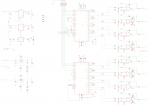
Not been an update in a while so here's a big one!
Boards arrived just over 2 weeks ago, but assembly takes quite a while for these, much more to solder than the CS3318 board! I am quite happy with the boards themselves, quality again is good, only I made the mistake of trusting an Eagle default package for the CS3318 footprint and the pads are too skinny to solder well. My custom footprint for the CS3318 was much nicer to work with, no idea why I didn't copy it over to the PCM4104 model!? Anyhow, it's far from impossible to solder, just a minor gripe.

I revised the filter design, didn't much like the peaking in group delay on the original one. The new one is flat GD out to 20kHz since it is a true Bessel response. <0.1dB down at 20kHz and a gentle roll-off after. During the build, capacitors were roughly matched, as a group, then the 470pF as accurate pairs.


Still needs a bit more flux removal/cleaning 😱


Been testing yesterday and today. Setup is I2S from a CM6631 USB audio interface over some salvaged internal USB cables to a stereo pair of the DAC at a time. All channels working fine! Listening through headphones only, with NE5532 to drive them.
Cannot hear any noise, even with the signal going directly to phones and using digital attenuation (0dBFS is a strong, headphone ruining, 3.75V RMS!). I then tried a 20dB gain stage after the DAC and with this in place a good listening level is -60dBFS, noise is fairly audible when paused/quiet sections but is benign hiss, nothing odd. In normal use with analogue post attenuator (-20dB) and signal around -10dBFS noise is obviously inaudible.
I tried to RMAA but I doubt its accuracy, coming out via one sound device and in on another. Perhaps it is ok, I don't like the distortion too much, it should be a few dB lower, but bear in mind this comes from the DAC, to an attenuator (full output will be too much for my soundcard input) through a buffer (OPA2134) and back, with unshielded cable along the way. But more likely, since it is distortion more so than noise, is poor delivery of I2S, because on the salvaged cable I have I2S data traveling on the shield! That's just how the plug was wired, real connection will be ribbon with ground between every data/clock line.

Anyhow, it really sounds immaculate on any channel pair, doesn't seem to do anything wrong. I'm still glad I opted to use a post analogue attenuator rather than the on-board digital attenuators, but in practice you could probably still get away with just the digital controls!
Boards arrived just over 2 weeks ago, but assembly takes quite a while for these, much more to solder than the CS3318 board! I am quite happy with the boards themselves, quality again is good, only I made the mistake of trusting an Eagle default package for the CS3318 footprint and the pads are too skinny to solder well. My custom footprint for the CS3318 was much nicer to work with, no idea why I didn't copy it over to the PCM4104 model!? Anyhow, it's far from impossible to solder, just a minor gripe.
I revised the filter design, didn't much like the peaking in group delay on the original one. The new one is flat GD out to 20kHz since it is a true Bessel response. <0.1dB down at 20kHz and a gentle roll-off after. During the build, capacitors were roughly matched, as a group, then the 470pF as accurate pairs.
Still needs a bit more flux removal/cleaning 😱
Been testing yesterday and today. Setup is I2S from a CM6631 USB audio interface over some salvaged internal USB cables to a stereo pair of the DAC at a time. All channels working fine! Listening through headphones only, with NE5532 to drive them.
Cannot hear any noise, even with the signal going directly to phones and using digital attenuation (0dBFS is a strong, headphone ruining, 3.75V RMS!). I then tried a 20dB gain stage after the DAC and with this in place a good listening level is -60dBFS, noise is fairly audible when paused/quiet sections but is benign hiss, nothing odd. In normal use with analogue post attenuator (-20dB) and signal around -10dBFS noise is obviously inaudible.
I tried to RMAA but I doubt its accuracy, coming out via one sound device and in on another. Perhaps it is ok, I don't like the distortion too much, it should be a few dB lower, but bear in mind this comes from the DAC, to an attenuator (full output will be too much for my soundcard input) through a buffer (OPA2134) and back, with unshielded cable along the way. But more likely, since it is distortion more so than noise, is poor delivery of I2S, because on the salvaged cable I have I2S data traveling on the shield! That's just how the plug was wired, real connection will be ribbon with ground between every data/clock line.
Anyhow, it really sounds immaculate on any channel pair, doesn't seem to do anything wrong. I'm still glad I opted to use a post analogue attenuator rather than the on-board digital attenuators, but in practice you could probably still get away with just the digital controls!
Attachments
-
 OctoDAC PCBs.jpg469.4 KB · Views: 755
 -
 Bessel schematic.png14.3 KB · Views: 708
 -
 Bessel filter at 110k.png12.4 KB · Views: 690
 -
 OctoDAC Complete Bottom.jpg110.5 KB · Views: 717
 -
 OctoDAC Complete Top.jpg147.2 KB · Views: 759
 -
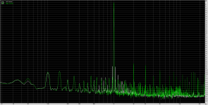 OctoDAC THD.png40 KB · Views: 682
 -
 OctoDAC Dynamic Range.png39 KB · Views: 100
 -
 OctoDAC Crosstalk.png17.9 KB · Views: 102
 -
 OctoDAC measurements crude.png35.5 KB · Views: 138
Member
Joined 2009
Paid Member
- Status
- Not open for further replies.
- Home
- Source & Line
- Digital Source
- New DAC PCB - Dual PCM4104 - 8 Channels