Hi.
I'm thinking about building new headphone amplifier around ADA4627-1. I would like to boost it's current capabilities using transistor in feedback loop, in similar way as in Heed Canamp (BD139).
1. ADA4627-1 or ADA4637-1 (above 6x gain).
2. +/-12 V power supply.
3. Small class A bias (~100mA).
What problems can I encounter? Is it good idea to use darlington with huge hFE, like CEN-U45 (25k hFE) - http://pl.mouser.com/ProductDetail/Central-Semiconductor/CEN-U45/?qs=sGAEpiMZZMshyDBzk1%2fWi36I9YbfeQLjfYfA1FLrHyo%3d
?
In the past I've only tried BD139 in feedback loop of OPA2604 without any problems, but it's hFE is way smaller.
Last question - if op-amp is not designed to drive low impedance load, like ADA4627-1, could I use small value resistors for the gain stage? I have very good metal foil resistors from RHOPOINT but in 100-200R range. Is darligton base high impedance, will it make possible to use low value resistors without stressing the op-amp?
With regards,
K.T.
I'm thinking about building new headphone amplifier around ADA4627-1. I would like to boost it's current capabilities using transistor in feedback loop, in similar way as in Heed Canamp (BD139).
An externally hosted image should be here but it was not working when we last tested it.
An externally hosted image should be here but it was not working when we last tested it.
1. ADA4627-1 or ADA4637-1 (above 6x gain).
2. +/-12 V power supply.
3. Small class A bias (~100mA).
What problems can I encounter? Is it good idea to use darlington with huge hFE, like CEN-U45 (25k hFE) - http://pl.mouser.com/ProductDetail/Central-Semiconductor/CEN-U45/?qs=sGAEpiMZZMshyDBzk1%2fWi36I9YbfeQLjfYfA1FLrHyo%3d
?
In the past I've only tried BD139 in feedback loop of OPA2604 without any problems, but it's hFE is way smaller.
Last question - if op-amp is not designed to drive low impedance load, like ADA4627-1, could I use small value resistors for the gain stage? I have very good metal foil resistors from RHOPOINT but in 100-200R range. Is darligton base high impedance, will it make possible to use low value resistors without stressing the op-amp?
With regards,
K.T.
Last edited:
Since your circuit operates at gain of 4.3X and the ADA4637 is only useful in circuits whose gain is 5X, you are stuck with the ADA4627.
The external transistor introduces some additional phase lag into the feedback loop, which increases the possibility of unstable oscillation by decreasing the Phase Margin. So you want a Darlington that won't add much phase lag, i.e., you want a fast Darlington. (It'll need to be 5 times faster with the '37 than with the '27). I'd recommend you choose one with fT > 16 MHz for the '27 opamp and fT > 80 MHz for the '37 opamp.
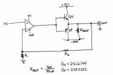
Since the opamp can drive 45mA and since you are happy with a 2A transistor, you only need an hFE of 80 or so. Maybe you can find a non-Darlington transistor that will do the job; it's likely you'll find higher fT in singles than in Darlingtons. For example the 2SC6144 might be a good fit.
The external transistor introduces some additional phase lag into the feedback loop, which increases the possibility of unstable oscillation by decreasing the Phase Margin. So you want a Darlington that won't add much phase lag, i.e., you want a fast Darlington. (It'll need to be 5 times faster with the '37 than with the '27). I'd recommend you choose one with fT > 16 MHz for the '27 opamp and fT > 80 MHz for the '37 opamp.
Since the opamp can drive 45mA and since you are happy with a 2A transistor, you only need an hFE of 80 or so. Maybe you can find a non-Darlington transistor that will do the job; it's likely you'll find higher fT in singles than in Darlingtons. For example the 2SC6144 might be a good fit.
Why not go with a CFP instead? Any reason you need that kind of current gain, especially with low-power where class-A biasing is a definite possibility?
Why not go with a CFP instead?
What would be a good(and readily available) pair of complementary transistors to use with the ADA4627-1?
I've made a very good 'phone circuit similar to that, but with a MOSFET instead. Base it on the old Siliconix current sink app circuit. See here- http://www.diyaudio.com/forums/chip-amps/163224-designing-super-low-distortion-headphone-amp.html
Last edited:
What would be a good(and readily available) pair of complementary transistors to use with the ADA4627-1?
I haven't looked. But for most headphone applications, at most you need your favorite medium-power driver transistor as your output transistor. And a clip-on heatsink.
I was under (false?) impression that higher hFE is better. So, 2SC6144 or BD139 instead of darlington? Maybe simple push-pull config instead of 1 transistor forced to operate in class A?
.png/220px-Pushpull_(English).png)
My power supply consists of LM317/337 regs + capacitance multiplier, I made fake darlington using bc550+BD139/bc560+BD140. Is there any reason to change it to real darlington in one package? I don't have 'scope, sound wise i couldn't find anything bad about it.
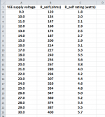
Ignore that 60R, this is too much, I would use max 50mA bias on cap multiplier.
My power supply consists of LM317/337 regs + capacitance multiplier, I made fake darlington using bc550+BD139/bc560+BD140. Is there any reason to change it to real darlington in one package? I don't have 'scope, sound wise i couldn't find anything bad about it.
An externally hosted image should be here but it was not working when we last tested it.
Ignore that 60R, this is too much, I would use max 50mA bias on cap multiplier.
Last edited:
My power supply consists of LM317/337 regs + capacitance multiplier, I made fake darlington using bc550+BD139/bc560+BD140. Is there any reason to change it to real darlington in one package? I don't have 'scope, sound wise i couldn't find anything bad about it.
Ignore that 60R, this is too much, I would use max 50mA bias on cap multiplier.
I thought we were discussing a headphone amp instead of a power supply?😕
I thought we were discussing a headphone amp instead of a power supply?😕
Yeah, we're talking about headphone amp, sorry for offtopic, I was currious about darlington.
So, what do You think about boosting the current output of ADA4627-1/4637-1? I don't want to use CFB buffer, just simple solution using transistors.
1. One NPN buffer biased into class A (using wirewound resistor or some nicer CCS),
or
2. NPN + PNP push-pull?
Maybe 3-4 stages of NPN/PNP combined using emitter resistors? That way there will be no need for a heatsink, I could just use bc550/bc560.
Headphones will range from 32 Ohm to 250 Ohm. I have some spare ADA46x7-1 chips, it would be nice to not over-complicate things but achieve good audio fidelity.
I'm not fixed about class A, from what I know crossover distortion in fast op-amps is not big deal.
Last edited:
Maybe you might want to try Douglas Self's "Crossover Displacement" idea.
He builds a Class-B power amplifier, but then forces a medium sized DC bias current to flow in the output stage, by simply connecting a current sink between the output and the minus supply. This runs the output stage in Class-A for small and medium-sized output currents (currents less than the DC sink). The output crossover, where NPN stops conducting and PNP starts conducting, is displaced. It's not at zero current, it's at DC_bias current. Self argues that this is less audible than crossover at zero. It's in his Audio Power Amplifier book, take a look.
A simplistic implementation is shown below. The arithmetic is also attached.
_
Attachments
Very interesting, where Can I read about it in more detail? Douglas Self Audio Power Amplifier?
I have Douglas Self Small Signal Audio Design, great book.
I have Douglas Self Small Signal Audio Design, great book.
Last edited:
I don´t get you.from what I know crossover distortion in fast op-amps is not big deal.
You strive for a fast, modern, low distortion Op Amp ... and then you *destroy* all that adding *guaranteed* horrible crossover distortion using unbiased output transistors?
I´m amazed.
As of power supply "sound" , I can´t hear DC (does anybody?) , nor do speakers reproduce it (besides an initial "thump!!" ) so not sure about what you mean.
I've made a very good 'phone circuit similar to that, but with a MOSFET instead. Base it on the old Siliconix current sink app circuit. See here- http://www.diyaudio.com/forums/chip-amps/163224-designing-super-low-distortion-headphone-amp.html
Is this the circuit you're referring to?
If so, what controls the offset at the outputs? Looks like the large 1M shunt resistor would make the impedance of the inputs mismatched resulting in a lot of offset.
Attachments

Last edited:
I don´t get you.
You strive for a fast, modern, low distortion Op Amp ... and then you *destroy* all that adding *guaranteed* horrible crossover distortion using unbiased output transistors?
I´m amazed.
If I hide output transistors inside feedback loop there should be no audible crossover distortion, right? This is the reason I started this thread, I have never tested push-pull inside feedback loop.
This is from OPA552 datasheet:
An externally hosted image should be here but it was not working when we last tested it.
It should work just fine, right?
I want to do something new just for fun, I'm bored with my ad8397 headphone amp, it's great but I have that "I must build something new" itch 😉

Maybe you might want to try Douglas Self's "Crossover Displacement" idea.
A simplistic implementation is shown below. The arithmetic is also attached.
Nice simple circuit. Thanks Mark for sharing it.
Is it best to mount both transistors on the same heatsink for thermal stability?
What value would you use for R2 if using the ADA4627-1?
That depends on two factors:If I hide output transistors inside feedback loop there should be no audible crossover distortion, right?
* opamp slew rate
* opamp open-loop gain bandwidth
The circuit you show is usable but by no means good, as it still has heavy gm variation over output swing. Basically the 100R (R2) fills in for the "dead zone".
If the 100R were not there at all, the dead zone would be in full effect, forcing the opamp output to slew rapidly from about -0.6 V to +0.6 V (or vice versa) each time the closed-loop output transitions through 0 V. This results in crossover distortion that doesn't really go away even at very low amplitudes.
With the resistor in, the opamp itself takes over for small output currents (<~6 mA peak), in which case the circuit acts like the buffer stage isn't even there. You'd be losing some loop gain as a result of the voltage divider involving 100R and the load, but it would be OK. At higher levels, the opamp still has to deliver no more than about +/- 6 mA (at which point the drop over the 100R becomes large enough for one of the transistors to turn on), which is an acceptable but by no means negligible load.
Do yourself a favour and implement some (semi-)proper biasing for the transistors. Two 1N4148 small-signal diodes in parallel with a 10 µF electrolytic across the bases and about a 2k2-3k3 resistor to either the negative or the positive rail would go a looooong way, while biasing the opamp output into Class A to boot. I'd use emitter resistors of like 1-4.7 ohms for an AB output headphone amp; adjust bias levels with a series resistor between the two diodes. (Common BD139/140s are a bit on the slow side and should really get some half-decent bias current. You may not want to spare as much as 30 mA, but 10 mA would be well spent. Aim for about 13 mV across each emitter resistor, i.e. 13 mA for 1 ohm or 6 mA for 2.2 ohms.)
While it's not terribly critical, the bias diodes are best placed directly at their respective transistors to exploit heat conduction through the legs (this is why I said any series resistor should go between the diodes); some further thermal coupling by establishing contact between the cases may be beneficial as well.
Last edited:
Do yourself a favour and implement some (semi-)proper biasing for the transistors. Two 1N4148 small-signal diodes in parallel with a 10 µF electrolytic across the bases and about a 2k2-3k3 resistor to either the negative or the positive rail
To clueless newbies who aren't sure which end of a soldering iron gets hot, I often recommend a different type of semi-proper biasing. It aims to reduces the width of the crossover deadzone, but not completely eliminate the deadzone. In other words, still class-B but a far less ugly class B. This is less prone to thermal destruction if the clueless newbie implements it cluelessly.
If the emitter followers are in TO92 packages:
- Two 1-amp silicon diodes (1N4002) in series. Gives slightly less than VBEnpn+VBEpnp
- A small signal silicon diode (1N4148) in series with a Germanium diode (1N34A)
- A small signal silicon diode in series with a small signal Schottky diode (BAT41-46, BAT85-86)
If the emitter followers are medium power devices in TO-126 packages:
- Two 3-amp silicon diodes (1N5404) in series
- A 3-amp silicon diode in series with a 1-amp Schottky rectifier (1N5817)
If the emitter followers are power transistors in TO-220 packages:
- A 3-amp silicon diode in series with a 1-amp Schottky rectifier
Why not use Nelson's self biasing follower with say a pair of 2SK1058 / 2SJ162 at 100mA ?
Also happens to be at zero tempco.
http://www.diyaudio.com/forums/atta...hammy20output_jpg_pagespeed_ic_4-mn-oxelx.jpg
Patrick
Also happens to be at zero tempco.
http://www.diyaudio.com/forums/atta...hammy20output_jpg_pagespeed_ic_4-mn-oxelx.jpg
Patrick
Well, I will design pcb for it so if I wanted something complicated I would just use output stage like in Lehmann BCL: http://cdn.head-fi.org/8/87/87579c0c_lovelycubecircuit01.jpg
I wanted something extremely simple and You suggest complex output stage.
Let's look at Douglas Self design from "Small Signal Audio Design" (I hope It's ok to put it here):
Is this really that bad thd? Can You hear 0.01% distortions?
I'm still leaning to one NPN inside the feedback loop, biased to class A using a simple resistor, or even simple CCS made from voltage regulator. If You have better ideas - go ahead, but make it simple, compact.
I wanted something extremely simple and You suggest complex output stage.
Let's look at Douglas Self design from "Small Signal Audio Design" (I hope It's ok to put it here):
An externally hosted image should be here but it was not working when we last tested it.
An externally hosted image should be here but it was not working when we last tested it.
Is this really that bad thd? Can You hear 0.01% distortions?
I'm still leaning to one NPN inside the feedback loop, biased to class A using a simple resistor, or even simple CCS made from voltage regulator. If You have better ideas - go ahead, but make it simple, compact.
Last edited:
- Status
- Not open for further replies.
- Home
- Amplifiers
- Headphone Systems
- Op-amp with darlington in feedback loop.