Hi anybody who's watching,
I'm building an implementation of Keith Snook's DCD-Mod4 on
"Class A dynamic biasing 80W amplifier PCB Quad 405"
boards from Jim's Audio on Ebay
Class A dynamic biasing 80W amplifier PCB Quad 405 2pcs | eBay
They are well made clones of M12368 pcb-s and can be relatively easily modified.
I'm prepping the boards now and and have them pretty much sorted, but see a couple of inconsistencies between Keith's schematic
http://www.keith-snook.info/amplifier-hifi-schematics/QUAD%20405%20schematic%20evolution.pdf (P.12)
and the illustrated implementations on his website.
QUAD 405-2 Amplifier Modification and Information
I'm wondering what the experts think:
1. The schematic shows R104/R105 feeding the bases of TR9 and TR10, but these are missing on the illustrated implementations. What do you think about their function?
2. The schematic shows R14 between the collector of TR1a and DUMPER ground, whereas the implementations connect TR1a collector to SIGNAL ground through R13
Conversely, the schematic shows R101 between SIGNAL ground and Q45(TR11) collector, whereas the implemetations have R101 connecting to DUMPER ground.
What are the consequences of each way of doing this?
Which is better?
Why the change?
Is the schematic an improvement on the implementations, or vice-versa?
Does in tot matter which way round as long as there's one connecting to each of the grounds?
Do the values of R101 and R13/14 depend on which ground is being used?
I'm eager to hear any views!
Cheers!
Well that's true, but that's the listing name of the boards on Ebay and I'm not here to pick holes in that.
Actually believe Bernd Ludwig described the current dumpers as class C, so I suppose technically its A/C, but that's an aside. Let's not drag the thread off-topic.
Regarding internal grounding:
Point 2: My bad. I was looking at an early revision of DCD Mod4 and see that Keith in a later revision changed R101 to go to DUMPER ground. This is in line with the illustrated implementation.
R14 is still replaced by R13 in the implementation, which does still go to signal ground.
This raises the general question of the ideal schema for internal grounding in amplifiers. Shopuld the direct 0V connection be reserved as far as possible for the dumper circuit, connecting all the previous points to the raised signal ground which is taken from the RCA input connectors (Tibi/Tvicol seems to d this in his Quaser rev. 13), or is it more complex than that? I see that Keith connects various points in the pcb to different ends of R2 in different revisions of the mods (see the evolution schematics from the link in the first post).
Ideally I'd like to avoid connecting signal ground to 0v at the RCA connector, but Keith mentions that this can case a 20mV offset at the output. Perhaps this can bi biased out somewhere else??
Others have mentioned connecting the input RCA shields to chassis at the input, but I'm not sure how this will work when I have separate PSU's with separate grounds for each channel.
perhaps we can also discuss pro-s and con-s of doing this.
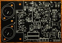
Prepped boards
I thought I'd show how far I've got. So far the boards are prepped by cutting and removing some of the traces on the back, removing unwanted links and unused copper surfaces:
and front showing wire links in place:
Differences from the implementation on Keiths site are:
R13 will be replaced by R114 which will go in the space vacated by R23 and will bridge TR1b base/TR1a collector and dumper ground.
The trace from TR108 collector and TR10 base has been removed to allow for R105.
The trace between R39 and D2 has been cut to allow R39 to be linked to the junction of C15/C16.
I have yet to decide whether to drill the extra hole needed to mount R3 vertically as suggested by Keith, or use the original hole and cut the track to Pin 2 of U1, bridging instead to the ground spur at the edge of the board.
Here is a photo of my intentions so far, showing front and back of board superimposed and components. I have yet to decide what to do in the space vacated by the crowbar fuses.
I will try to make a clearer drawing of this when I have time.
I thought I'd show how far I've got. So far the boards are prepped by cutting and removing some of the traces on the back, removing unwanted links and unused copper surfaces:
An externally hosted image should be here but it was not working when we last tested it.
and front showing wire links in place:
An externally hosted image should be here but it was not working when we last tested it.
.Differences from the implementation on Keiths site are:
R13 will be replaced by R114 which will go in the space vacated by R23 and will bridge TR1b base/TR1a collector and dumper ground.
The trace from TR108 collector and TR10 base has been removed to allow for R105.
The trace between R39 and D2 has been cut to allow R39 to be linked to the junction of C15/C16.
I have yet to decide whether to drill the extra hole needed to mount R3 vertically as suggested by Keith, or use the original hole and cut the track to Pin 2 of U1, bridging instead to the ground spur at the edge of the board.
Here is a photo of my intentions so far, showing front and back of board superimposed and components. I have yet to decide what to do in the space vacated by the crowbar fuses.
An externally hosted image should be here but it was not working when we last tested it.
I will try to make a clearer drawing of this when I have time.
Last edited:
And here's an easier to read mockup. Please disregard component values for the moment and let me know if you find any mistakes.
Green markings on front of board
Blue markings on back
Black marks are cut traces
Red and dark blue blobs are connection points for + / -50V supply lines
The green blob is a possible connection point to 0V and speaker ground, but this might not be possible depending on what goes on around the fuse / C15/C16 space.
An externally hosted image should be here but it was not working when we last tested it.
Green markings on front of board
Blue markings on back
Black marks are cut traces
Red and dark blue blobs are connection points for + / -50V supply lines
The green blob is a possible connection point to 0V and speaker ground, but this might not be possible depending on what goes on around the fuse / C15/C16 space.
Last edited:
QUAD405 is not class a. it is class b.
Is it not a Current Dump design where the main amplifier is in fact a Class A but only up to a few watts then the current dump comes into play to boost the power.
All I remember is that they do sound pretty awful when compared to todays technology.
Class A and/or B?
Even if you supplied enough current? Current rate for this setup is +- 50 volts. How much VA can you push it?Is it not a Current Dump design where the main amplifier is in fact a Class A but only up to a few watts then the current dump comes into play to boost the power.
All I remember is that they do sound pretty awful when compared to todays technology.
BOM
Learnincurve. Would you have, for this project, a BOM for the components? I just received PCBs where I have to follow the silk screen information. I would also like to compare the latest BOM to what's on the PCBs. Thanks. I also wanted to say that I got a pair of finished Quads from Asia through ebay with D1047/TIP42 outputs. I hooked one up with a 2A 24ct, through a pair of old 18000uF, iPod input and I am surprise. Can't wait to do the modification on our boards with a proper power supply and with some canned outputs transistors for the black PCBs.And here's an easier to read mockup. Please disregard component values for the moment and let me know if you find any mistakes.
An externally hosted image should be here but it was not working when we last tested it.
Green markings on front of board
Blue markings on back
Black marks are cut traces
Red and dark blue blobs are connection points for + / -50V supply lines
The green blob is a possible connection point to 0V and speaker ground, but this might not be possible depending on what goes on around the fuse / C15/C16 space.
Attachments


Learnincurve. Would you have, for this project, a BOM for the components? I just received PCBs where I have to follow the silk screen information. I would also like to compare the latest BOM to what's on the PCBs. Thanks. I also wanted to say that I got a pair of finished Quads from Asia through ebay with D1047/TIP42 outputs. I hooked one up with a 2A 24ct, through a pair of old 18000uF, iPod input and I am surprise. Can't wait to do the modification on our boards with a proper power supply and with some canned outputs transistors for the black PCBs.
Hi Spurlte.
Those finished boards look interesting. What revision are they based on? Do you have the link?
I'll PM you with the other information.
Here's an updated image:
An externally hosted image should be here but it was not working when we last tested it.
I was looking at this circuit, lifted from the Quad 606:
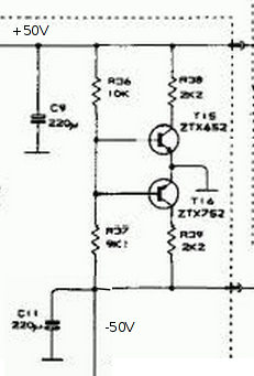
I created it in EveryCircuit (Android App) and see that by changing the values of R36 and R37 we can adjust the + and - rail offsets (to give for example +57.8V / -53.4V as for the 606).
Can anyone think of any use for this in the 405? Do we get any theoretical stability advantage from employing such a circuit (with the same value for R36/R37 to give 0 offset)?
I also see that C9 and C11 are pretty massive electrolytics compared to the 100nF or even 1uF of C15/C16 in the 405. Is there any advantage to adding larger electrolytics across C15/C16 and what would a good bypassing arrangement be here (eg. 220uF Electro + 1uF Polyprop. +???). I'm asking as I now have a bit of space on the boards having removed the fuses.
Last edited:
This will only work if it has a resistance in the supply lines to work against.
Is there?
What does this do in the larger context of the amp - as shown it doesn't really do anything.
Jan
Is there?
What does this do in the larger context of the amp - as shown it doesn't really do anything.
Jan
voltage division...
I don't think this can help with stability issues with 405 builds. IIRC This circuit was used in some later quad amps (606, 707 etc) because there was no transformer center tap. The PSU caps act as a voltage divider giving a virtual 0v with a low dynamic impedance. The exact rail voltages will depend on current draw from the respective circuit halves etc AFAICT the circuit shown was designed to drain current from an overcharged PSU cap during long periods of output asymmetry, keeping the two halves within a well defined voltage range. Unless the capacitors are rated for the full rail voltage, if the asymmetrical signal persists, and the excess voltage/current is not drained a vigorous failure of a PSU cap is likely ;-)
I think that if the values chosen in the draining circuit are changed to try and create a new voltage difference between the top and bottom halves, the value of the PSU caps should be changed to also divide out to the required difference, or the relatively small transistors shown here or the resistors in series will pop.
Good luck.
Stuart
I was looking at this circuit, lifted from the Quad 606:
An externally hosted image should be here but it was not working when we last tested it.
I created it in EveryCircuit (Android App) and see that by changing the values of R36 and R37 we can adjust the + and - rail offsets (to give for example +57.8V / -53.4V as for the 606).
Can anyone think of any use for this in the 405? Do we get any theoretical stability advantage from employing such a circuit (with the same value for R36/R37 to give 0 offset)?
I also see that C9 and C11 are pretty massive electrolytics compared to the 100nF or even 1uF of C15/C16 in the 405. Is there any advantage to adding larger electrolytics across C15/C16 and what would a good bypassing arrangement be here (eg. 220uF Electro + 1uF Polyprop. +???). I'm asking as I now have a bit of space on the boards having removed the fuses.
I don't think this can help with stability issues with 405 builds. IIRC This circuit was used in some later quad amps (606, 707 etc) because there was no transformer center tap. The PSU caps act as a voltage divider giving a virtual 0v with a low dynamic impedance. The exact rail voltages will depend on current draw from the respective circuit halves etc AFAICT the circuit shown was designed to drain current from an overcharged PSU cap during long periods of output asymmetry, keeping the two halves within a well defined voltage range. Unless the capacitors are rated for the full rail voltage, if the asymmetrical signal persists, and the excess voltage/current is not drained a vigorous failure of a PSU cap is likely ;-)
I think that if the values chosen in the draining circuit are changed to try and create a new voltage difference between the top and bottom halves, the value of the PSU caps should be changed to also divide out to the required difference, or the relatively small transistors shown here or the resistors in series will pop.
Good luck.
Stuart
Thanks Stuart for the explanation.
In fact I'm going to use the 606 method of creating a virtual centre tap for the PSU. In doing so I remove the need for the DC clamp circuit and on-board rail fuses, fusing instead the AC output of each trafo (I'm using independent toroids for each channel). Here' a little diagram of the intended supply:
An externally hosted image should be here but it was not working when we last tested it.
If anyone has clear opinions about where the quality of components (caps) is important for Mod-4 please send me a private message.
How's it going?
Hi Lerningcurv,
Just wondering how the build went overall?
Are you happy in general with the results and what would you do differently next time?
I've had an early Quad 405 for a while and want to do similar mods and I'm starting from scratch rather than touching the original. Have you since come across boards which didn't need as much modification, though these don't need too much?
Did you get a good response to your question about where to spend the money on capacitors?
Most importantly, are you happy with the sound?
Cheers!
Rob
- Status
- Not open for further replies.
- Home
- Amplifiers
- Solid State
- Quad 405 - DCD–Mod4 (Keith Snook)