Hi all, have been lurking here a long time and have learned a ton from you all. Hoping you can help me answer some questions I can't seem to find answers to. Please let me know if this is the wrong forum to post this in.
I've been looking at the Mackie ProFX mixer schematic to understand the gain structure. From the user perspective, the line inputs feature a gain control that goes from -20dB to +40dB, with another +10dB available on the fader. Looking at the schematic, I can see that there is a voltage divider at the input that cuts -20dB, followed by the gain circuit that appears (per my simulations) to add a variable amount of gain between +6dB and +56dB. There is another gain stage near the fader that adds another +6dB, the fader itself is just a voltage divider. There's probably some other attenuation in there, so I see how it more or less all adds up to what is advertised on the front panel. I have questions about how this gain circuit actually works though:
1) This circuit (page 2 of linked schematic) is located before the circuit that unbalances the signal, so it is effectively duplicated for both + and - inputs, and therefore requires two transistors (IMBT4403) and two op-amps (NJM4580). I've simulated half and the gain is exactly the same, so I'm wondering why they did it this way. Is it so CMRR could be used to reject some of the noise introduced by the gain stage? Would it be much noisier single-ended?
2) I vaguely grasp that the transistor in the feedback loop is being used as a current amplifier to increase loop current and thus the gain of the op amp, but I would like to better understand the physics/math and be able to calculate gain and other circuit characteristics.
3) How does the gain pot actually vary the gain of the circuit? It is in series with a 470uF cap, bridging the emitters of both transistors. I presume that it allows some current to leak so the gain is lower, but again, I would love some clarification on how it actually accomplishes that. Also, that cap seems to cause some low-end roll-off (-3dB at 30Hz, see attached frequency response); I would have expected the 3dB point at a lower lower-frequency. Maybe they boost bass later in the circuit?
4) Would this perform similarly with different op amps/transistors? Is there anything special about the choice of components for this purpose? I simulated using 2N3906 and NE5532 since I didn't have models for these components. Would they perform well in this circuit?
Thank you, I look forward to your thoughts!
Steve
Attachments

Hi Steve
This is a circuit I've not seen before - and I may have gotten it wrong.
But let me take a stab at it - not trying to answer all your questions:
The circuit looks a lot like the standard instrumentation amplifier (with 3 opamps), but with the input applied at the "wrong" opamp inputs.
Now, If you take for example the circuitry around U2, the voltage across R2 will be kept at a constant matching the voltage across R9 - 2.96V.
This will give a constant current of 0.97mA through Q1 which the feedback loop will maintain.
This will result in that any voltage on the input changing the voltage across the GAIN control and thus change in current through same will be matched by an equal, but opposite change of the current though R4.
As I get it, this will get the same result for gain as the standard 3 opamp instrumentation amplifier.
To determine the math for calculating the gain, the output impedance of the input generators and the value range of the GAIN needs to be known, but I do not know who to read the simulation tool you are using - so could you explain this?
Cheers, Martin
Hi Martin.
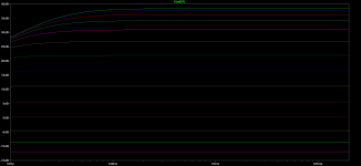
Thank you for your response, I will need to spend some more time with it to absorb it fully. The simulation is in LTSpice. The GAIN control is a 10K audio taper pot, the output I shared is a logarithmic sweep of that value showing the gain of the circuit at different values. The output impedance of the input generators is 18.2K, which was determined from earlier stages of the schematic - with R6 and R8 it creates the -20dB pad I mentioned in the original post.
Thank you for your response, I will need to spend some more time with it to absorb it fully. The simulation is in LTSpice. The GAIN control is a 10K audio taper pot, the output I shared is a logarithmic sweep of that value showing the gain of the circuit at different values. The output impedance of the input generators is 18.2K, which was determined from earlier stages of the schematic - with R6 and R8 it creates the -20dB pad I mentioned in the original post.
This looks like a modified instrumentation amplifier.
1) Putting most of the gain in the buffer section before the diff-amp is common to boost the CMRR of the input by the gain as the common mode is not amplified. I do not think it has to do with the noise in the gain stage in particular.
For the other questions: Can you confirm the direction of increasing resistance on the gain pot. From my quick glance, it looks like highest gain would happen at the lowest resistance setting. Indeed, I expect the two opamps before the diff-amp to behave somewhat like voltage buffers with Rgain open circuit...