Hello everyone!
I am trying to come up with schematics for the universal input buffer that would use balanced and unbalanced connections for the input. I have placed a switch at the end after the op-amplifiers, but not sure if that will work well?
I also added power regulators LM317, LM337 that will allow to power this from the DC supply of 15V to 40V with center ground.
Idea behind this board was - to be able to combine it with any power amplifier boards out there. For example, LM3886, TDA7396, or discrete amp like JAT501. Since it is a buffer, you can use chip amp in inverted schematics.
Something similar is done by Tom from Neurochrome - https://neurochrome.com/collections/buffers-preamps
However, those boards don't come with input connectors, so I wanted to add those.
Any thoughts or input will be greatly appreciated,
Pavlo


Attachments
Last edited:
Why not just make a differential input and ground the negative input when the source is unbalanced?
Yes, D4 is going to fry the circuit that way round!
Not sure I understand the layout - why regulators not at the edge where they can have heatsinking? Why not arrange layout to match function? Arranging all the resistors and caps like that is maybe risking issues due to stray impedances - layout should follow function and the signal path(s).
Where is the high-speed decoupling for the opamps? They need this to behave according to datasheet.
Perhaps because the performace will be a little worse, inheriting the extra noise of the 10k differential stage but with 6dB less signal level to help counter it? And you don't get the source-selection switch either?Why not just make a differential input and ground the negative input when the source is unbalanced?
Last edited:
On the face of it: they drop at-most 25V at 20mA, so may dissipate 0.5 Watts, which the naked TO-220 can do fine if not crowded by tubes.why regulators not at the edge where they can have heatsinking?
The one op-amp diff-input is suitable for economy mixer line input but isn't something to brag about. D.Self has a chapter on good diff line inputs. IMHO he goes a bit too far beyond.... but he does consult with high-class makers, and you can pluck something mid-chapter if you don't want to get crazy.
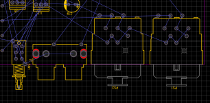
PCB has not been designed yet. That arrangement is to show idea with the input connectors and switch being on the edge of the board, ready to be mounted in a predrilled side of the amp case.Yes, D4 is going to fry the circuit that way round!
Not sure I understand the layout - why regulators not at the edge where they can have heatsinking? Why not arrange layout to match function? Arranging all the resistors and caps like that is maybe risking issues due to stray impedances - layout should follow function and the signal path(s).
Where is the high-speed decoupling for the opamps? They need this to behave according to datasheet.
Perhaps because the performace will be a little worse, inheriting the extra noise of the 10k differential stage but with 6dB less signal level to help counter it? And you don't get the source-selection switch either?
Where is the high-speed decoupling for the opamps? They need this to behave according to datasheet.
Are those between V+ and V- , pin 8 and 4?
Or you talking about one in feedback loop?
I have made some changes to the schematics.
Apparently I need DC blocking capacitors on all four outputs of the opams - that is for the signal selector switch to be working silently. R17, R18, R19, R20 provide DC offset to the opamps' inputs and can leak some of it to the output.
As far as the input level, I was thinking +4 dBu or 1.228 Vrms for both balanced and unbalanced inputs.
Balanced inputs can be improved by implementing unity gain instrumentation amplifier. Improved CMRR will be -63dB and noise -111.6 dBu. Will it be worth it though? Any thoughts?
PCB is not finished yet!
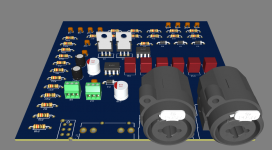
I attached 3d model just to illustrate the concept. Schematics is work in progress and will change a lot, so I did not want to draft the PCB layout yet. 3d model shows those inputs and switch very well - also output terminals are on the opposite side - those locations will probably be kept in the final PCB layout.
Attachments
Attached are calculations that were done to see CMRR improvements.
With gain_1 of 4x and gain_2 of 0.25, CMRR improved by 13dB
With gain_1 of 8x and gain_2 of 0.1322, CMRR improved by 17.7
All resistors are selected for total unity gain of the circuit.
 dB
dB
With gain_1 of 4x and gain_2 of 0.25, CMRR improved by 13dB
With gain_1 of 8x and gain_2 of 0.1322, CMRR improved by 17.7
All resistors are selected for total unity gain of the circuit.
If you haven't read Bruno Putzey's article 'the G word' I would recommend googling that and going through it. He presents a circuit in that which, whilst possibly overkill for your requirements will give some food for thought. Various threads on it as quite a few people use this as their line stage.
Of course all depends what you want from this board...
Of course all depends what you want from this board...
On the supply next to the chip, like with any high speed decoupling.Are those between V+ and V- , pin 8 and 4?
Or you talking about one in feedback loop?
BTW your new version has a time constant of 10s for the input capacitors which doen't right to me - that's a long time for a DC offset at switch-on to die down. C31 and C32 can be 10uF in that circuit I think. Even at 20Hz 10uF is 800 ohms or so, so I think you can live with the CMRR due to capacitor mismatch?
If you like clipping.I wonder if I can set gain to 10 on the first two and 0.1 on the third one?
"+4" is a concept. Equipment is often worked much harder. I have seen/heard a feed clipping a +23dBu output. We usually take XLR signals through a PAD, not an amplifier.
My plan is to draft it in LTspice and then dial in all of the caps values.On the supply next to the chip, like with any high speed decoupling.
BTW your new version has a time constant of 10s for the input capacitors which doen't right to me - that's a long time for a DC offset at switch-on to die down. C31 and C32 can be 10uF in that circuit I think. Even at 20Hz 10uF is 800 ohms or so, so I think you can live with the CMRR due to capacitor mismatch?
Found it. Interesting read.If you haven't read Bruno Putzey's article 'the G word' I would recommend googling that and going through it. He presents a circuit in that which, whilst possibly overkill for your requirements will give some food for thought. Various threads on it as quite a few people use this as their line stage.
Of course all depends what you want from this board...
Attachments
Assuming +4.0 dBu input signal we get 1.228 Vrms at the input. That is split between two differential signals gives 0.614 Vrms.
Instrumentation amplifier posted earlier has a gain of 7.6666 on the first stage. That gives output of 0.614 * 7.6666 = 4.7072 Vrms on the outputs of the first stage. I am assuming that NE5532 needs to be driven to 15Vrms to be clipping? Because it's power supply is +-15V?
Simulation shows 13V clipping though.
Increasing power supply to +-18V gives headroom all the way to 16V ish.
Assuming +4.0 dBu input signal we get 1.228 Vrms at the input. That is split between two differential signals gives 0.614 Vrms.
Instrumentation amplifier posted earlier has a gain of 7.6666 on the first stage. That gives output of 0.614 * 7.6666 = 4.7072 Vrms on the outputs of the first stage. I am assuming that NE5532 needs to be driven to 15Vrms to be clipping? Because it's power supply is +-15V?
Simulation shows 13V clipping though.
Increasing power supply to +-18V gives headroom all the way to 16V ish.
Unless otherwise noted, RMS levels in audio are related to sine waves. The peak voltage of a sine wave is square root of two times the RMS value. The op-amp output stage needs some voltage, typically 2 V and maximally 3 V for an NE5532, so its output can go to +/- 12 V ... +/- 13 V at +/- 15 V supply. The largest possible RMS level is then 12 V/sqrt(2) ~= 8.48528 V minimum, 13 V/sqrt(2) ~= 9.19239 V typical.
More importantly, as PRR wrote, that +4 dBu is only a nominal level for professional equipment, not a maximum level.
I will have three possible sources for the signal:
Focusrite Scarlett 2i4 1st gen:
Unbalanced - max output +5.5 dBu or 1.46 Vrms
Balanced - max output +10 dBu or 2.45 Vrms
Rolls RM67
Balanced TRS jack
Output level max +17 dBV or 20 dBu or 7Vrms
Vizio E55-E1
Unbalanced RCA phono
I am assuming 0.775mV or 0 dBu
- Home
- Source & Line
- Analog Line Level
- Universal buffer with balanced/unbalanced switch


