Hi guys, Ive been banging my head in it for a few hours and I was wondering, can I calculate the components around the tube based on the gain I want. Everywhere I looked, the calculations for the gain at the very end where Ive already determined all the components and cant change anything anymore. I have an ECC85 and I want it to have a gain of 10. You can say it wont see any load because the next stage I plan on bootstapping and itll have >1Mohm impedance. How can I do the calculations?
For a triode gain stage with bypassed cathode resistor
Rp=A*rp/(mu-A)
where Rp is the plate load resistor,
rp is the triode's plate resistance,
mu is the triode's amplification factor, and
A is the desired gain
Rp=A*rp/(mu-A)
where Rp is the plate load resistor,
rp is the triode's plate resistance,
mu is the triode's amplification factor, and
A is the desired gain
To adjust a single stage gain there are at least two alternatives:
- attenuator at the input
- use of negative feedback
Both can be calculated.
- attenuator at the input
- use of negative feedback
Both can be calculated.
You want a gain of 10 from a triode that has a mu=55?
I would probably use some form of feedback if this valve is the only option. Or just pick a more appropriate triode with a low to medium mu.
I would probably use some form of feedback if this valve is the only option. Or just pick a more appropriate triode with a low to medium mu.
ECC85 is osc/mixer from old FM radios--It was custom designed for that purpose.....
There's better valves around for what you want than this old RF valve. A better choice for the gain you're looking for would be ECC82......
There's better valves around for what you want than this old RF valve. A better choice for the gain you're looking for would be ECC82......
Last edited:
Except that ECC82 /12AU7 still has too high gain.
NFB or voltage divider is required to get gain of 10.
NFB or voltage divider is required to get gain of 10.
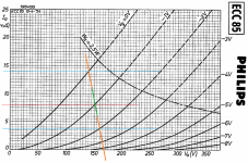
Easy, look at the Philips chart.Except that ECC82 /12AU7 still has too high gain.
NFB or voltage divider is required to get gain of 10.
If you take away the cathode decoupling (50µF) the gain is 10x and less distortion.
Mona
Attachments
Or use a split anode resistor and take output from the junction - anode load and attenuator combined.
There is no simple way of getting a good amplification stage with a gain of 20% of the valve mu. All possible methods involve compromise: low input impedance or high output impedance or high distortion. You either need to choose a more suitable valve or adopt a more complicated circuit (probably involving two valves and feedback).
There is no simple way of getting a good amplification stage with a gain of 20% of the valve mu. All possible methods involve compromise: low input impedance or high output impedance or high distortion. You either need to choose a more suitable valve or adopt a more complicated circuit (probably involving two valves and feedback).
Hi guys, Ive been banging my head in it for a few hours and I was wondering, can I calculate the components around the tube based on the gain I want.
No, you can't. Hollow state design isn't done by formula like it is for solid state. If you wanted a BJT voltage amp where AV= 10, that's simple:
AV= RC/(RE + re) and done. (There's a comparable formula for FETs as well)
These kinds of formulas don't apply to hollow state. There are various network formulae, but they do you no good if you don't know what values to use with them, and VT characteristics like gm and rp can vary widely with plate current. That leaves design by loadlines, and the main criterion for performance is low distortion, and you take the gain you get. If you have to have some specific gain, about the only thing you can do is split the plate resistor into RP1 and RP2 and scale them to tap off the required voltage such that vo/vi= 10.
Of course, there are some universals. One is that the lighter the load, the better the linearity, as the delta-I is less for any given delta-V. In solid state design, you generally don't worry about it since transistors have way more gain than VTs, and you don't require output matching xfmrs since transistors are already Lo-Z devices, so you can have enormous open loop gains and big enough feedback factors to linearize them.
I found in ltspice it was hard to alter gain of a valve/tube stage.
The only method that made much difference was adding/removing cathode bypass capacitor.
After that its down to attenuators in the circuit.
Or a transformer.
The only method that made much difference was adding/removing cathode bypass capacitor.
After that its down to attenuators in the circuit.
Or a transformer.
Graphical methods can be useful sometimes. Just for fun, I drew in a load line that yields 10X gain centered on Va=150 by stretching it across the zero and -2V grid lines where they cross Va=140 and Va=160. That load turns out to be about 1.92K, which puts B+ voltage at 166V for 8mA of bias current. The green line represents anode excursion for 1Vpp input, and you can see from its unequal length on either side of the operating point that some distortion will occur. A hotter operating point would yield less distortion. Does that help?


- Status
- Not open for further replies.
- Home
- Amplifiers
- Tubes / Valves
- Voltage gain triode
