SA 2012 finished
Attachments
-
 Detail Front.jpg70.6 KB · Views: 1,002
 -
 Schalter.jpg50.1 KB · Views: 269
 -
 Unterseite schräg.jpg128.5 KB · Views: 291
 -
 Unterseite offen.jpg122 KB · Views: 266
 -
 Oberseite offen2.jpg114.6 KB · Views: 255
 -
 Oberseite offen leicht von oben.jpg113.5 KB · Views: 260
 -
 Detail Ecke 2.jpg60.3 KB · Views: 871
 -
 Detail Ecke 1.jpg55.7 KB · Views: 892
 -
 Detail oben.jpg106 KB · Views: 937
 -
 Detail Front groß.jpg74.8 KB · Views: 960


Well done! Congratulations!
Do you have the FFT:s between different channels, say best channel and worts channel?
Would be interesting to see, what causes the difference in performance?
Do you have the FFT:s between different channels, say best channel and worts channel?
Would be interesting to see, what causes the difference in performance?
Well done! Congratulations!
Do you have the FFT:s between different channels, say best channel and worts channel?
Would be interesting to see, what causes the difference in performance?
Mostly noise from toroid radiation. The measurement setup was also quick'n dirty. The results in the lower wattage range are not representative as the distortion analyzer wasn't running at its sweet spot.
Read the graphs "as good as or better".
BR, Toni
P.S.: Maybe "Tiroler" will bring me the amplifier again for detailed measurements...
OMG! Now that is enviable craftsmanship. You must have a whole workshop! I have to outsource all the machining. I don't trust myself to put even just 2 holes in exactly the right place!
Thanks! For such testing I do not have the necessary know how or/and equipment. Toni did it with HP Spectrum Analyzer; a Douglas Self “Distortion magnifier” coupled to the Levear analyzer you can see in the picture. We got just readouts with two zero´s behind the decimal, so it´s fine for me 😀. Meanwhile Toni´s lab is equipped with absolute state-of-the-art units as he always strives for very best performance of his circuit designs. The subtle visible difference in the measure graphs I cannot explain, but he chimed in meanwhile...
I must say that I took quite an effort to create a good layout, e.g. well separating mains cables from audio signal carrying cables, extreme shielding in order to separate the audio circuits from the power supply, keeping cabling as short as possible etc. You can see this in the images and you may want to have a look at the attached CAD file. The MOSFET´s were closely matched, but there are always minor tolerances in parts like the caps of the compensation circuit or other parts of a circuit. Maybe you also want to check back with the datasheet of the LME49830.
I must say that I took quite an effort to create a good layout, e.g. well separating mains cables from audio signal carrying cables, extreme shielding in order to separate the audio circuits from the power supply, keeping cabling as short as possible etc. You can see this in the images and you may want to have a look at the attached CAD file. The MOSFET´s were closely matched, but there are always minor tolerances in parts like the caps of the compensation circuit or other parts of a circuit. Maybe you also want to check back with the datasheet of the LME49830.
Attachments


Hi Tyroler & Astx,
Are you willing to share info (just LME board schematics + PCB design) for this interesting project?
I still have some 49830's lying around waiting to be used.
Thanks,
Jacques
Are you willing to share info (just LME board schematics + PCB design) for this interesting project?
I still have some 49830's lying around waiting to be used.
Thanks,
Jacques
SA2012: Schematics
Note: Schematics are free to use only for non commercial DIY projects.
WARNING: the circuit is using and providing very high AC and DC voltages and is therefore very dangerous and can be lethal. I am not responsible for any costs, damage and/or injury using these schematics. Do not use this schematics if you do not have the necessary experience and knowledge.
BR, Toni
Attachments

Note: Schematics are free to use only for non commercial DIY projects.
Thanks Toni!
SA2012: Gerber
a single sided pcb will do it:
Note: Gerbers are free to use only for non commercial DIY projects.
BR, Toni
a single sided pcb will do it:
Note: Gerbers are free to use only for non commercial DIY projects.
BR, Toni
Attachments

Last edited:
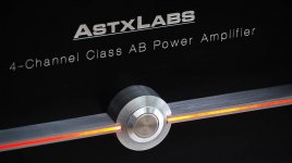
Parts of the front and the transformer covers are made of stainless steel in order to create some highlights and a more interesting design. The switch is mounted in special part which I fabricated out of a massive stainless steel rod with a lathe. At the sides of this part there are slots. Both side stripes are made of stainless steel that I laser-welded together at the end. In between there are thin (1mm) acrylic glass stripes embedded. The light comes from LED´s at the side of the central switch. That was very tricky to make. A much better and way easier to make version would be milling a thin slot through the front plate and use something like this at the rear side of the front plate.
SA2012: Schematics
Power supply for one or two channels.
Note: Schematics are free to use only for non commercial DIY projects.
WARNING: the circuit is using and providing very high AC and DC voltages and is therefore very dangerous and can be lethal. I am not responsible for any costs, damage and/or injury using these schematics. Do not use this schematics if you do not have the necessary experience and knowledge.
BR, Toni
Attachments

SA2012: Gerber
a single sided pcb will do it:
Note: Gerbers are free to use only for non commercial DIY projects.
BR, Toni
a single sided pcb will do it:
Note: Gerbers are free to use only for non commercial DIY projects.
BR, Toni
Attachments

Last edited:
- Status
- Not open for further replies.
- Home
- Amplifiers
- Chip Amps
- SA 2012 amplifier - LME49830