After my Parasound P/LD 1100 pre-amp had a slight problem I decided to check the capacitors in my other devices as well.
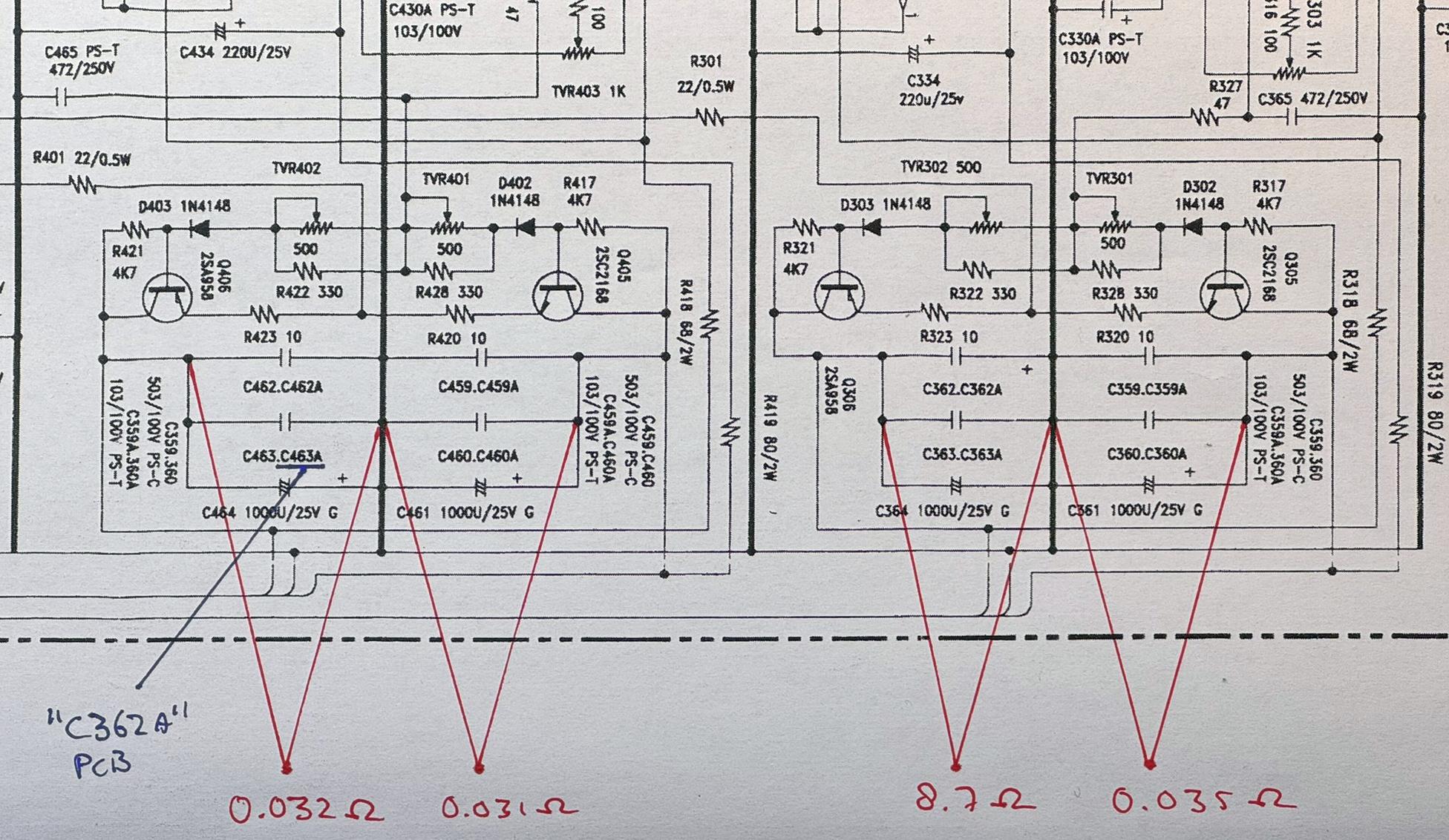
While checking the D/AC 1100's capacitors with my blue-esr meter I noticed that measuring the ESR on C364 and it’s bypass capacitors (C362 / C362A / C363 / C363A) gave a much higher result (8.7 ohms) then measuring the other capacitors that are placed in the same way (around 0.03x ohms). After removing the PCB from the housing I noticed that the traces around C364 have a different layout than C464 / C 461 and C361.
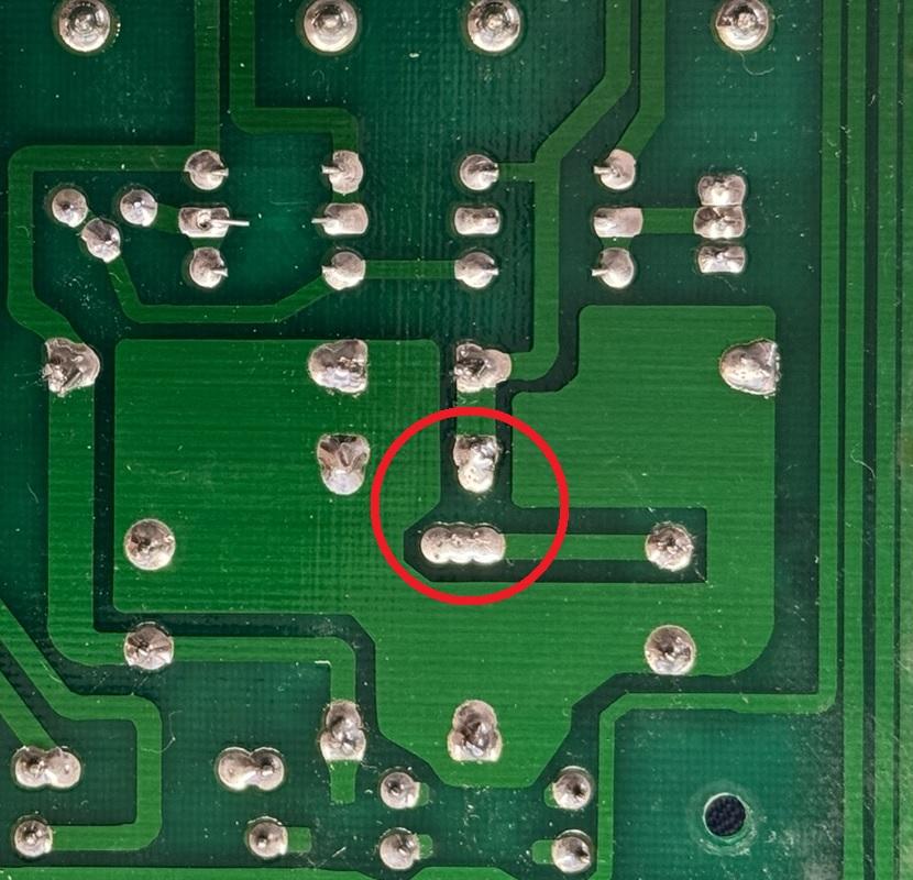
While measuring DC resistance from C364 to the empty solderpad in the red circle I measure around 10 ohms which corresponds with R232.
Now I'm no professional, but in my opinion it appears that Parasound made a mistake in the PCB layout and I think the traces with the red circle around them should be connected?
What do you think about it?
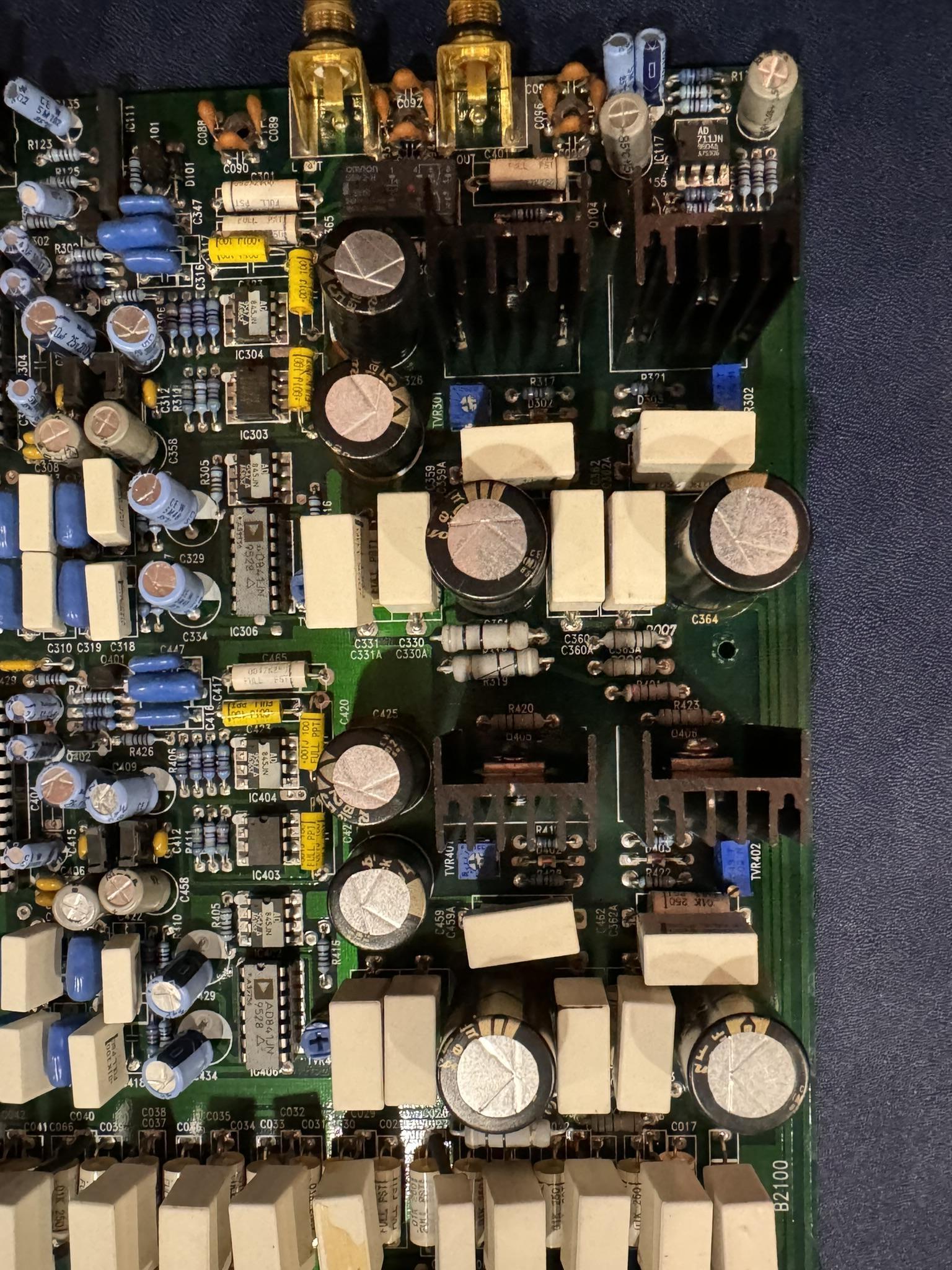
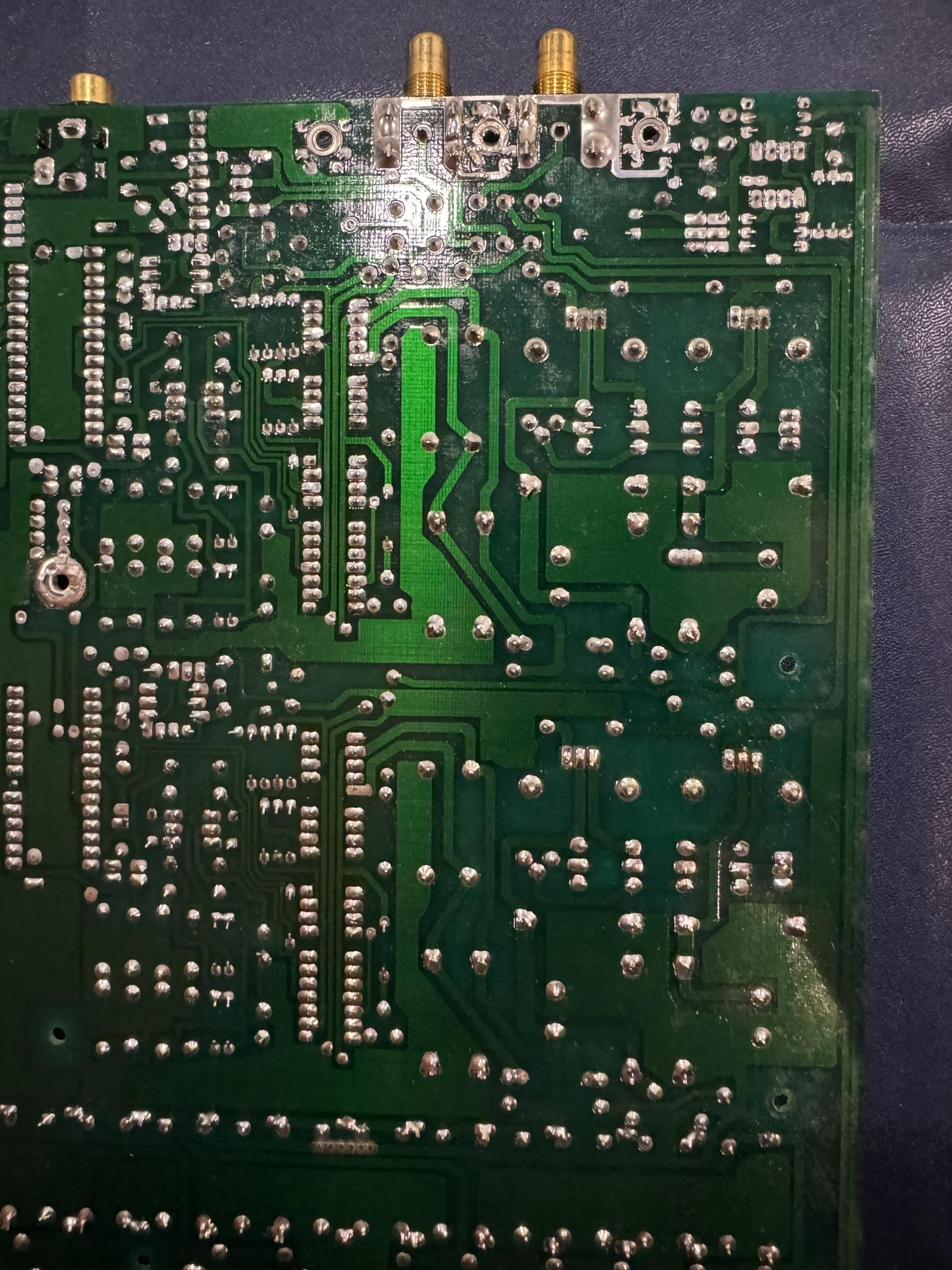
Without having a board in front of me to spin around and look at in detail its very difficult to say (working from pictures is notoriously difficult... remember you have it in front of you  )
)
What I can tell you is that it is absolutely normal to see changes in production to board layouts and the like that are not reflected in the service manual. It happens everywhere in all types of equipment.
What I can tell you is that it is absolutely normal to see changes in production to board layouts and the like that are not reflected in the service manual. It happens everywhere in all types of equipment.
Thanks for the reply, I didn't realize that would be an option to double check it.
Unfortunately I don’t have a service manual or service bulletins, the only thing I have is a schematic.
I can’t imagine that a manufacturer like Parasound made a design fault like this. But, as (almost?) all electrolytic caps are bypassed I think it is hardly noticeable during testing.
Yes, I understand it’s very difficult, especially as this is a dual layer board.Without having a board in front of me to spin around and look at in detail its very difficult to say (working from pictures is notoriously difficult... remember you have it in front of you)
What I can tell you is that it is absolutely normal to see changes in production to board layouts and the like that are not reflected in the service manual. It happens everywhere in all types of equipment.
Unfortunately I don’t have a service manual or service bulletins, the only thing I have is a schematic.
I can’t imagine that a manufacturer like Parasound made a design fault like this. But, as (almost?) all electrolytic caps are bypassed I think it is hardly noticeable during testing.
I did the measurements as suggested by Rayma. C362 and C363 are sharing the same solder pad so the results are exactly the same.
Collector Q306 – C362 neg. 0,04 Ω
Collector Q306 – C363 neg. 0,04 Ω
Collector Q306 – C364 neg. 10,13 Ω
To do an extra check I also measured from the collectors of transistors Q305 / Q405 and Q406 to C361 / C461 and C464. These measurements show the same problem.
Q306 Collector – C364 neg. 10,12 Ω
Q305 Collector – C361 pos. 0,06 Ω
Q406 Collector – C464 neg. 0,08 Ω
Q405 Collector – C461 pos. 0,07 Ω
These measurements confirm my suspicion that something is wrong. I'm thinking of connecting the PCB traces and then using the Blue ESR meter to see if I get the same results as the surrounding components. Another option is to lift one leg of R323 and do the measurements again. If the measurements that showed ~10Ω before are open circuit that confirms my thoughts.
Last edited:
Can you visually check the node for the negative lead of C364 on the other side, to see if anything is connected to those pads?
It's unlikely, but you should check. Then lift one end of that 10 ohm resistor and measure to confirm.
Then go ahead and add a jumper, and verify that now C364 measures with a low ESR.
It's unlikely, but you should check. Then lift one end of that 10 ohm resistor and measure to confirm.
Then go ahead and add a jumper, and verify that now C364 measures with a low ESR.
Last edited:
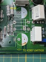
Removed C360/C360A, C363/C363A , C361 and C364 to get a better overview of the top side of the PCB. The negative terminal of C364 is connected to IC007 (supply) and by a VIA from the bottom side to the top side to R318 which corresponds with the schematic. See the attached picture.
But somehow I think I am making a mistake with the 10 Ω coming from R323 as that is connected to the emitter of Q306. I can’t explain where the 10 Ω I measure between C364 neg. and C362/C363 neg originates.
After some staring at the schematic I noticed R007, it is draw in the power supply part of the schematic but it's the resistor under R318 in the picture. going to try what happens if I lift that one tomorrow and compare it to it's neighbour circuit.

Attachments
I can’t imagine that a manufacturer like Parasound made a design fault like this. But, as (almost?) all electrolytic caps are bypassed I think it is hardly noticeable during testing.
They won't be any different to all the mainstream brands (such as Sony, Hitachi, Technics, Rotel etc etc etc) where this kind of thing is commonplace. Problems in actual use by customers are flagged and revisions made to later production runs.
The capacitors measure 0.034 Ω for C364 and 0.038 Ω for C361. Capacity and dissipation factor don’t show abnormalities either.Ok, that 10R is certainly coming from somewhere.
If you measure ESR directly across C364, from one end to the other, what do you get?
If I measure “ESR” on the PCB from the pads of C364 I measure 0.15 Ω, on the pads of C361 I measure 10 Ω. If I measure ESR on the negative side of C363/C363A and the positive side of C364 I also measure 10 Ω. R006 and R007 limit the current in the positive and negative 18 volt rail going to C361 and C364. The 10 Ω ESR is measured through the remaining caps. Those measurements initially strengthened my suspicions
But then I decided to measure the DC resistance from IC006 (LM7818) and IC007 (LM7918) to C361 and C364 and those measurements show that C364 has both positive and negative connected directly without going through R007.
- Measuring DC resistance from the output pin of IC006 (LM7818) to the positive pin of C361 gives a reading of ~10 Ω. This is because of R006 being in series.
- Measuring DC resistance from the GND pin of IC006 to the negative pin gives a reading of 0.09 Ω.
- Measuring DC resistance from the output of IC007 (LM7918) to the negative pin of C364 gives a reading of 0.08 Ω. This should be ~10 Ω because it should be connected in series via R007.
- Measuring DC resistance from the GND of IC007 (LM7918) to the positive pin of C364 gives a reading of 0.09 Ω.
To make sure it wasn’t by design I also measured the outputs from the other channel IC008 (LM7818) to C461 and IC009(LM7918) to C461 and those both have a 10 ohms resistor in series.
In my opinion the only way to modify it so it’s exactly the same as in the schematic is to cut the trace between the output of IC007 and the negative pin of IC007 and then connect the solder pads so the negative pin of C364 is connected behind IC007. Then it’s exactly the same as the schematic and the other three voltage regulators.
In my opinion the only way to modify it so it’s exactly the same as in the schematic is to cut the trace between the output of IC007 and the negative pin of IC007 and then connect the solder pads so the negative pin of C364 is connected behind IC007. Then it’s exactly the same as the schematic and the other three voltage regulators.
Oops, I made a typo in the above text, behind IC007 should be behind R007.
I have drawn a small schematic to compare the situation as is should be according to the schematic and the situation as it is in real life.
I don't have enough knowledge to analyze the consequences of C364 being before R007 instead of being in series with it. In the original schematic it limits the charging current to C364. In the current situation in limits the amount of current leaving C364. What consequences does this have for the circuit behind it? I would suggest that fast current demands are being limited possibly resulting in clipping?
And then, how to fix it, and should I fix it? As it is a double layer board I can’t easily cut a trace and move R007. I could however remove R007 at it’s current location, place a jumper and lift pin 3 of IC007 and put R007 in series with it. Visualy not the nicest solution but then the circuit is exactly like the schematic and the other 3 regulators.
Well... this appears like a classic case of 'where more seems better'.
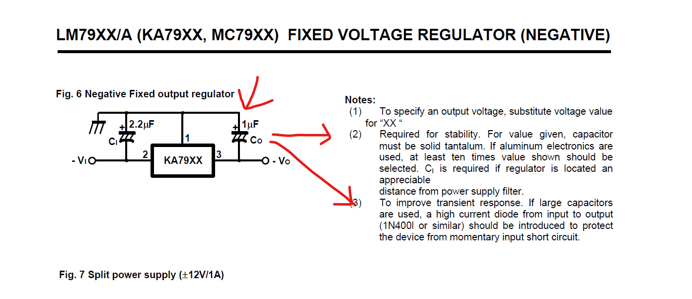
Adding lots of capacitance to the output of a linear regulator like the 78 and 79 series parts isn't always a smart move and the reason why is that big caps change the behaviour of how the regulator operates in the face of varying load currents. A regulator needs to respond quickly to any change in loading and if that change in demand is met by a cap rather than the regulator itself you can end up with poor regulation.
As always in these cases, the data sheets show how it should be done. Note how small the recommended caps really are.
There is also another possible reason.
Adding parallel small value caps such as C362 and C363 means they appear also in parallel with the electrolytic in the first version and that could be problematic given that electrolytics are 'pretty poor' at high frequencies because of highish self inductance and variable esr. They are also not very consistent one to another as they age. It is remotely possible that the combination triggers some kind of low level very high frequency instability in the regulator as a result of an ill defined resonant load. Separating the electrolytic from the other caps would stop that.
Adding lots of capacitance to the output of a linear regulator like the 78 and 79 series parts isn't always a smart move and the reason why is that big caps change the behaviour of how the regulator operates in the face of varying load currents. A regulator needs to respond quickly to any change in loading and if that change in demand is met by a cap rather than the regulator itself you can end up with poor regulation.
As always in these cases, the data sheets show how it should be done. Note how small the recommended caps really are.
There is also another possible reason.
Adding parallel small value caps such as C362 and C363 means they appear also in parallel with the electrolytic in the first version and that could be problematic given that electrolytics are 'pretty poor' at high frequencies because of highish self inductance and variable esr. They are also not very consistent one to another as they age. It is remotely possible that the combination triggers some kind of low level very high frequency instability in the regulator as a result of an ill defined resonant load. Separating the electrolytic from the other caps would stop that.
I am familiar with the fact that by design these regulators should be used with much lower capacitance. My question isn’t about that, I don’t want to change the design, I want that both channels have the same configuration / behavior. Regarding the aging, all the caps, the large electrolytic’s and the smaller bypass caps measure fine for as far as I’m able to measure them with a Der EE DE-5000.
I’m just wondering what the consequences are that C364 is in a different configuration then C361, C461 and C464 while they have exact the same function. And how I can solve this in an easy way.
I’m just wondering what the consequences are that C364 is in a different configuration then C361, C461 and C464 while they have exact the same function. And how I can solve this in an easy way.
Fair enough.My question isn’t about that, I don’t want to change the design, I want that both channels have the same configuration / behavior.
It still leaves unanswered as to whether this is a deliberate design change or an error. You (none of us) just don't know.
The impact of the difference would probably be non measurable because as drawn you have the same resistor in series with the regulator output with no take off points before. That means the DC voltage should be identical in both case. The only difference is in the supply impedance and transient capability but if the current draw is a constant then that should not be an issue.
I can say from experience that sometimes very odd and strange issues can appear in production equipment and that the 'fixes' used by manufacturers can be equally odd and strange.
Ultimately its up to you whether to alter the design to match the other side.
- Home
- Source & Line
- Digital Line Level
- Parasound D/AC 1100 HD - strange measurement / fault?
