At 50vdc there should be a minimum of 0.6mm between the +/- power supply rails to ground.
As an example a 2oz 5mm track width at a 22 degrees temp rise is rated at approx 8.7amps (subject to other PCB parameters).
Saturn PCB Design have a nice free PCB software tool that has all these calculations - https://saturnpcb.com/saturn-pcb-toolkit/
As an example a 2oz 5mm track width at a 22 degrees temp rise is rated at approx 8.7amps (subject to other PCB parameters).
Saturn PCB Design have a nice free PCB software tool that has all these calculations - https://saturnpcb.com/saturn-pcb-toolkit/
Last edited:
High current density perhaps. Current in a series circuit is the same everywhere. And high current density means higher stray inductance as well as self-heating.In the post #35 above, even with the large traces, isn't it true that the thinnest section of a trace is the funnel for high current?
My KiCad defaults wasn't appropriated then...
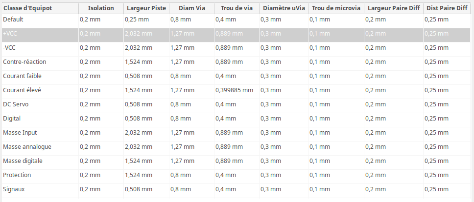
Following the most conservative suggestions above, I modified the minimum spacing to 1.2mm for power rails, ground and high current traces.
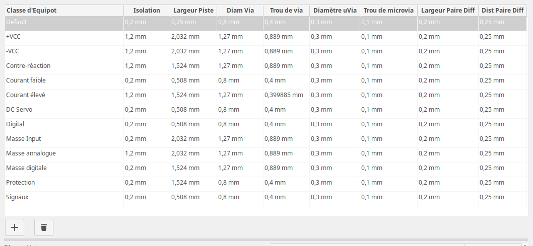
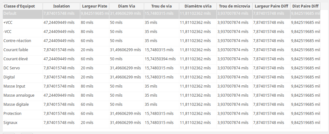
In mils...
We have this expression in French :
Following the most conservative suggestions above, I modified the minimum spacing to 1.2mm for power rails, ground and high current traces.
1.2 mm would be the minimum spacing assuming standard PCB material without a conformal coating.
In mils...
We have this expression in French :
100 fois sur le métier, remettez votre ouvrage!
10 times over, rework your work
@Sevy, the said 1.2mm is creepage distance for conductors without a conformal coating, or solder mask, and is not from a standard suiting domestic electronic device such as an audio amp.
With presence of a conformal coating, IPC-2221B recommends 0.4mm minimum @101-150V, see column B4 in the attached. And 0.4mm is what we have in my day-job products that need to be CSA-ed.
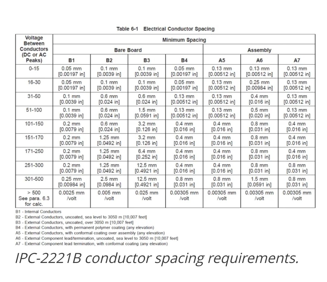
With presence of a conformal coating, IPC-2221B recommends 0.4mm minimum @101-150V, see column B4 in the attached. And 0.4mm is what we have in my day-job products that need to be CSA-ed.
From the MOSFET Output datasheet for the ECX10N20 and ECX10P20, the maximum continuous drain current is 8A.
I always use 2 oz Cu PCB with solder mask. Your 1.2mm rail spacing above is without coating, right?
I ask PCBWay what is the thickness of 2 oz Cu. They answered 2 * 0,035mm - 0,07mm. I had also some tools calculators with KiCad based on the IPC 2221. If I configured these values I get these results from the B4 column, 31 to 100V:
B4 - External conductors, with permanent polymer protective coating (any altitude)
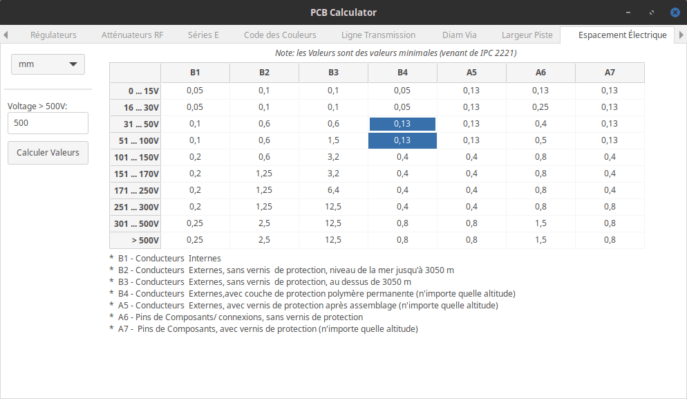
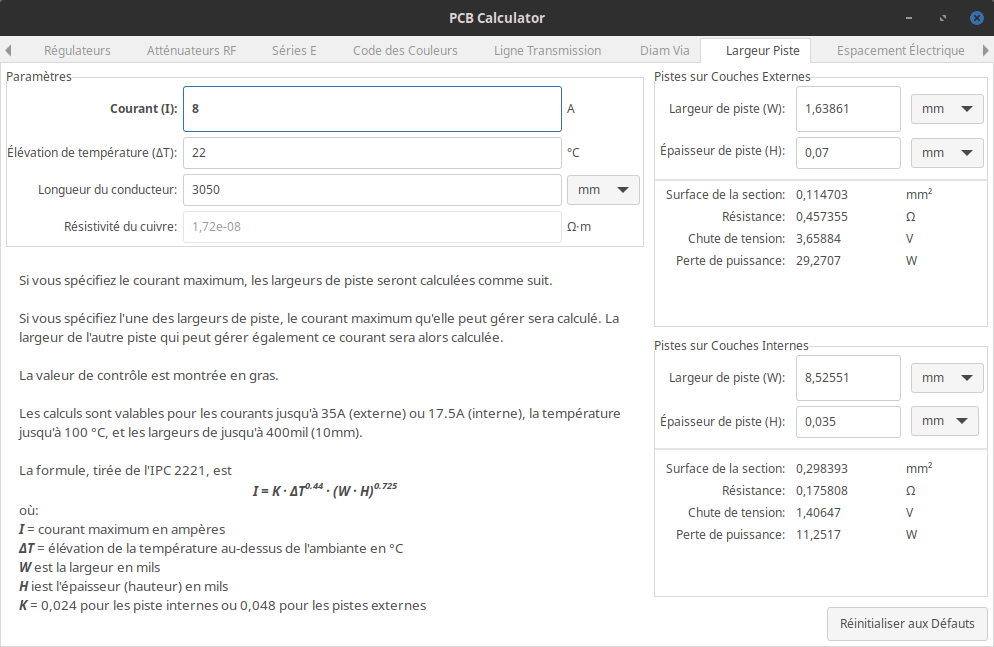
So I should be ok with 1,64mm traces width, spaced from 0,13mm one to each other. am I right?
I always use 2 oz Cu PCB with solder mask. Your 1.2mm rail spacing above is without coating, right?
I ask PCBWay what is the thickness of 2 oz Cu. They answered 2 * 0,035mm - 0,07mm. I had also some tools calculators with KiCad based on the IPC 2221. If I configured these values I get these results from the B4 column, 31 to 100V:
B4 - External conductors, with permanent polymer protective coating (any altitude)
So I should be ok with 1,64mm traces width, spaced from 0,13mm one to each other. am I right?
IPC-2221 is obsolete for pcb conductor current calculations, its been replaced by IPC-2152I had also some tools calculators with KiCad based on the IPC 2221
So...
Seeing that the highest voltage I got from my actual toroidal transformer was 49.something VDC, and that my theoretical design was done for 50 VDC, I guess that with your suggestion of 0,4mm nattawa and my calculation at 1,3mm above, I wasn't so bad with a default 0f 0,2mm of space violation limit after all, no?
@Indiglo your post just came in after my writing. What would be your suggestions based on the IPC-2152, 2 oz Cu, 50 VDC maximum, with permanent solder mask?
That's right. Also, it may be worth noting that the IPC-2221B recommended minimum creepage distances are NOT mandatory enforced, but rather more of voluntary guideline nature. Breaching the IPC-2221B does not mean immediate failure of a PCB/product design, but that PCB/product design becomes subjected to hipot tests and/or accelerated failure mechanism tests in order for it to be safety-certified.So...
Seeing that the highest voltage I got from my actual toroidal transformer was 49.something VDC, and that my theoretical design was done for 50 VDC, I guess that with your suggestion of 0,4mm nattawa and my calculation at 1,3mm above, I wasn't so bad with a default 0f 0,2mm of space violation limit after all, no?
I use Linux but do have a dual booting partition with Windows 11
FYI, I also dual boot and just installed pcb toolkit in linux (opensuse tumbleweed) using wine, seems to run okay.
Also in pcb toolkit, goto program options under Tools in the menu and change the colour theme to either windows or windows 10, the dark colour schemes were unreadable using Wine.
Last edited:
Yes, after having installed wine and the tool successfully, I figured out that bug myself with the dark setting ;-)FYI, I also dual boot and just installed pcb toolkit in linux (opensuse tumbleweed) using wine, seems to run okay.
Also in pcb toolkit, goto program options under Tools in the menu and change the colour theme to either windows or windows 10, the dark colour schemes were unreadable using Wine.
I started over my board layout checking progressively my traces length in the tools and finally, with my board at 10 inches wide, I still can use the 80 mils trace width I was using for the ground and the rails over a 10 inch length without problem... See below, I can travel more than 8A over 10 inches!
This seems backwards.Ground:
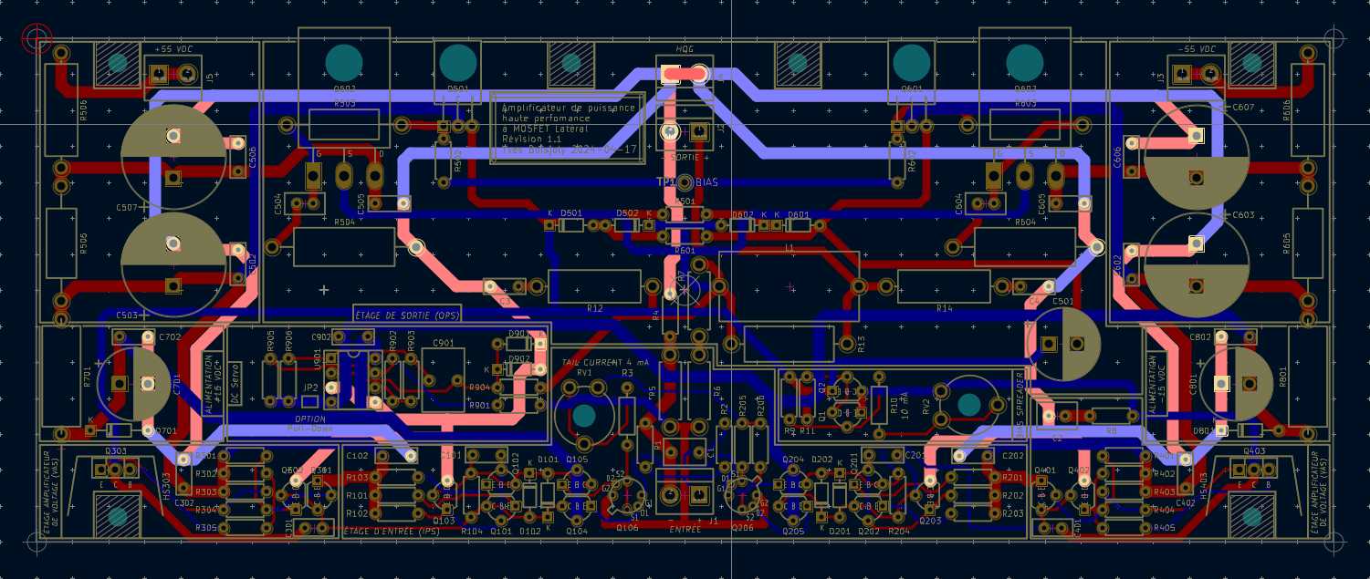
Unless you know you need something different, ground should probably be a plane by default, not traces.
Then "scrape away" thin lines of copper to add insulation. Use online calculators to estimate parasitic capacitance and inductance. If the empty insulating areas between traces are too big, you may unwittingly create RF antennae. If they are too small, you may slow down critical parts of the amplifier with a few extra pico Farads of capacitance. The latter is likely to be a much smaller problem, but it could be important in for the feedback loop.
Ouf!Unless you know you need something different, ground should probably be a plane by default, not traces.
It seam that a lot of peoples have different view of how to route an amplifier. I remember having ask if a ground plane would be adequate and some answered me back the contrary.
I feel that I am turning around with this board layout. Every time I modify it to respect some good advises, someone else came in with other good advises that make me go back to square one.
Star grounds were probably fine, and more fun to debug, in the days when every sqr cm of board space cost a dollar, but a ground plane is certainly safer.
There are caveats -- remember to add 'spokes' to the component pads to avoid soldering issues. Anyway, that's just my suggestion.
There are caveats -- remember to add 'spokes' to the component pads to avoid soldering issues. Anyway, that's just my suggestion.
- Home
- Amplifiers
- Solid State
- A Lateral MOSFET Power Amplifier Design Version 1.1