Not yet, next week I will order parts and if I'm lucky (i.e. enough free time) maybe next weekendDid you already try the new version?
In that case(balanced output), you need four AD811s, as I will use in my new DAC with two PCM1794s.It is indeed a simple yet promising lil circuit to be tried.
Btw it seems clear @grunf you are using it as single ended output, what would actually be best way to use it in case of balanced output chips? Maybe using a small resistor or grounding the chip negative output?
The dimensions are 70*30mm, if I used SMD electrolytes the PCB would be even smaller, but I deliberately want TH UKZ at least while there are still some to buy.Hi grunf
Can I ask the dimensions of the board?
I got everything ordered and want to get the board made.
Klaus
Igor
Attachments
I agree, in my case the regulator and power supply are much more complicated and expensive than the IV stage itself.@Radian, considering the lead spacing on the 8 pin dips is 2.54mm I'd estimte the board to be 55 ~ 60 ish mm long.
But the AD811 has low PS rejection so you need to use a very low noise high quality power supply. The power supply is where all the space in this design will be,
I can get a 160mm X 100mm board made for
€26. 105um traces instead of 35um.
We can get 6 boards onto this area.
I need two for a differential setup.
grunf you can get two just for the cost of shipping if you like.
Shipping takes 7 days after payment.
Gerbers would be nice but pic works to.
We can up the area and put more boards on to it if interest exists.
Greets Klaus
Thank you for your answer.In that case(balanced output), you need four AD811s, as I will use in my new DAC with two PCM1794s.
Not been clear sorry, I am using a balanced output chip (a pcm1794 per channel) into a single ended integrated amp (currently with passive iv stage). Since a single ended output is needed, what would be the best way to menage the negative ouput of the dac chip using the ad811 single ended output from the positive?
Grunf, I think you have mis-interpreted the application of that 1kohm resistor..I understood correctly, it should look something like this, four AD811 for two PCM1794.
The original Jung scheme is applying it !behind the feedback node. (below)
Your schematic means that you have eliminated the 0 ohm virtual ground that the Dac output wishes to see and now there is 1kohm I/V resistor in place, with some Volt of voltage compliance to tolerate for the Dac..
Attachments
@grunf, just found this thread, watching with intrest.
Had you thought of using some JFETS in the front end? - the same as the CEN IV https://www.diyaudio.com/community/threads/folded-cascode-cen-iv-with-fixed-rails.389776/
Had you thought of using some JFETS in the front end? - the same as the CEN IV https://www.diyaudio.com/community/threads/folded-cascode-cen-iv-with-fixed-rails.389776/
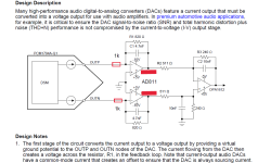
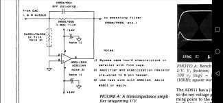
AD811 is not for voltage out dacs, a classic VFA op amp is sufficient thereIs the AD811 only good for I/V duty or can it be used on voltage out dacs as well?
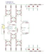
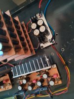
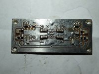
Today I finished the prototype PCB for IV with AD811 but this time everything with SMD components except four 100uF/50v ukz and two AD811 with heatsinks.
For the first time I used DALE PNM non-magnetic series instead of RN60, and instead of polystyrene and polypropylene TH capacitors I used non-magnetic SMD COG capacitors. AD811 is soldered direct on the PCB.
So far I can say that in this application the PNM is much better than the RN60.
For the first time I used DALE PNM non-magnetic series instead of RN60, and instead of polystyrene and polypropylene TH capacitors I used non-magnetic SMD COG capacitors. AD811 is soldered direct on the PCB.
So far I can say that in this application the PNM is much better than the RN60.
Attachments
Have you tried AD811? It's not without reason that Walt Jung made an IV for TDA1541 with AD811.I've never been convinced that the 811 is a good choice, whereas the AD844 is, for current output dacs.
- Home
- Source & Line
- Digital Line Level
- AD811 as I/V stage for current DACs (and test some other op amps including Burson Audio op amps as I/V)