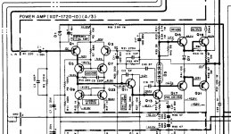
Hoping that someone with greater knowledge of amplifier circuits than myself can have a look. This is the amplifier in a Sherwood S-9180CP receiver, @1981. It is a BOTL unit. There is no provision for adjusting DC offset. Other corners may have been cut, I don't know.
The amp sounds fine, very nice actually for 18wpc. However, DC offset is hovering around 60mV in both channels. This is what I am hoping to fix.
I have recapped and installed new, hFe matched diff pair transistors (2sa970BL). I know that is the first thing that would be suggested for addressing offset issues. New 4 transistors all measured around 404 hFe, original pairs were off by around 40 and 50. Actually, the channel with one of the mismatched original pairs DC offset was lower (21mV) than with the new matched pair, the other original channel had higher offset (73mV). Now, both channels' offset is nearly identical with the matched new 2sa970's.
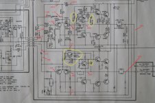
Do the voltage readings marked on the schematic below look normal for this topology? Some things that I do not understand are:
1) why is there +dcV on the base of the input transistor of both differential pairs (Q501 L&R)?
2) Why do DC voltage readings switch from positive to negative on either side of the series NFB resistors (R511 L&R)?
3) On both C502L (&R), there is +.73dcV on one side (and I see where that comes from), but also +.169 (+.167) on the other side of those caps, which I do not understand.
4) The components I have circled in yellow form a type of circuit that I have not seen in other schematics. Does this circuit have something to do with controlling DC offset?
Perhaps this amp is completely healthy, and @ 60mV DC offset is normal due to design limitations? Or maybe something is amiss?
In the schematic below all voltages are marked in dcV, not mV. Thanks in advance...
The amp sounds fine, very nice actually for 18wpc. However, DC offset is hovering around 60mV in both channels. This is what I am hoping to fix.
I have recapped and installed new, hFe matched diff pair transistors (2sa970BL). I know that is the first thing that would be suggested for addressing offset issues. New 4 transistors all measured around 404 hFe, original pairs were off by around 40 and 50. Actually, the channel with one of the mismatched original pairs DC offset was lower (21mV) than with the new matched pair, the other original channel had higher offset (73mV). Now, both channels' offset is nearly identical with the matched new 2sa970's.
Do the voltage readings marked on the schematic below look normal for this topology? Some things that I do not understand are:
1) why is there +dcV on the base of the input transistor of both differential pairs (Q501 L&R)?
2) Why do DC voltage readings switch from positive to negative on either side of the series NFB resistors (R511 L&R)?
3) On both C502L (&R), there is +.73dcV on one side (and I see where that comes from), but also +.169 (+.167) on the other side of those caps, which I do not understand.
4) The components I have circled in yellow form a type of circuit that I have not seen in other schematics. Does this circuit have something to do with controlling DC offset?
Perhaps this amp is completely healthy, and @ 60mV DC offset is normal due to design limitations? Or maybe something is amiss?
In the schematic below all voltages are marked in dcV, not mV. Thanks in advance...
Attachments
Last edited:
Nothing to fixHoping that someone with greater knowledge of amplifier circuits than myself can have a look. This is the amplifier in a Sherwood S-9180CP receiver, @1981. It is a BOTL unit. There is no provision for adjusting DC offset. Other corners may have been cut, I don't know.
The amp sounds fine, very nice actually for 18wpc. However, DC offset is hovering around 60mV in both channels. This is what I am hoping to fix.
Perfectly normalI have recapped and installed new, hFe matched diff pair transistors (2sa970BL). I know that is the first thing that would be suggested for addressing offset issues. New 4 transistors all measured around 404 hFe, original pairs were off by around 40 and 50. Actually, the channel with one of the mismatched original pairs DC offset was lower (21mV) than with the new matched pair, the other original channel had higher offset (73mV). Now, both channels' offset is nearly identical with the matched new 2sa970's.
Do the voltage readings marked on the schematic below look normal for this topology?
Those are PNP transistors and like any bipolar need current flowing into their base for normal operation.Some things that I do not understand are:
1) why is there +dcV on the base of the input transistor of both differential pairs (Q501 L&R)?
Being PNP current flows "downwards" through ground reference resistors so base is more positive than ground.
Because base side is more positive than the one connected to speaker out. See above2) Why do DC voltage readings switch from positive to negative on either side of the series NFB resistors (R511 L&R)?
See above explanations.3) On both C502L (&R), there is +.73dcV on one side (and I see where that comes from), but also +.169 (+.167) on the other side of those caps, which I do not understand.
No.4) The components I have circled in yellow form a type of circuit that I have not seen in other schematics. Does this circuit have something to do with controlling DC offset?
Completely healthy.Perhaps this amp is completely healthy, and @ 60mV DC offset is normal due to design limitations? Or maybe something is amiss?
Thank you for that informative (and well organized) response JMFahey!
That is good news...
But it seems there might be an opportunity to lower DC offset. One of the originally mismatched diff pairs was producing lower offset than the same channel with a matched pair.
I know this may sound screwy, and I have never heard of anyone intentionally mismatching diff pairs. But maybe I could reproduce what was happening in that one channel? I have a lot of KSA992F sitting around that I could experiment with...
Matching the LTP transistors is a relative term. By matching, here it actually means offsetting the individual Hfe measurements to achieve the lowest acceptable offset and this is done commercially too. 30mV would be absolutely fine, though. Perhaps 60mV is a tad irritating to our sense of correctness but won't upset much, despite alarmist fears about bass driver centering.
If you can't get close enough with the range of relacement transistor Hfe you have, you can Google "how to fix DC offset with no trimpot" for a bit more advice and on the reasons why this happens and how to adjust in general.
If you can't get close enough with the range of relacement transistor Hfe you have, you can Google "how to fix DC offset with no trimpot" for a bit more advice and on the reasons why this happens and how to adjust in general.
Last edited:
Thank you Ian.
Just makes a slight pop when powering up or down. There is no speaker relay. If I can do something about minimizing that pop I want to try. Putting a lot of time into this unit now. When it is closed up I will be on to other things, lol. If I can get it down to 30mV from 60 I will be happy with that. I did not know that "...offsetting the individual Hfe measurements..." was something that was done commercially.
My transistors are from Digikey, Mouser, or BDent...so if they are not genuine then a lot of us are in trouble, lol. I have a lot more of the KSA992 than the 2sa970 though. If experimenting I don't want to waste the 2sa970 parts.
Any harm in using KSA992 to permanently replace 2sa970 in the diff pairs?
Last edited:
Just to add.....
1. Parts circled in yellow form a soft start circuit. Should reduce speaker pop on turn on.
2. Input differential pair is unbalanced by design. The 10K tail resistor has about 20 volts across it - this means 2 mA total for the pair. With the 1.2K load resistor on Q501, that means it will be developing enough voltage to start turning the VAS on with 0.5 mA through Q501. So statically, you will have about 0.5 mA through Q501 and 1.5 mA though Q502. That mismatch can certainly produce the output offset you are seeing. If you wanted to 'play', you could try changing R508 to 15K and see what happens to the offset. I wouldn't suggest any higher as it might reduce the amp stability of input signal handling capabilities.
But I agree that the 60 mV output offsets are fine.
....Perhaps this amp is completely healthy, and @ 60mV DC offset is normal due to design limitations?...
Bingo.
It is a low-price product. "Much better" designs were well known, but the original buyer of this product didn't pay for it. It does seem to balance-out the various errors well. 60mV is NOT a problem--- 0.000,4 Watts of DC will not bother the assumed 18 Watt woofer sold with this amplifier. 1V would not be a big deal, though most such amps do better so that would invite investigation.
You "could" trim-out the offset on the bench. It won't stay trimmed with temperature and other effects. The offset is the sum of several factors which can't all drift the same way.
Button-up and enjoy it.
@Ylli - Soft start circuit... it did seem like the speaker pop was milder than I would have expected. And thanks for the analysis on current through those transistors. Makes sense now that it has been pointed out to me.
@PRR - Thanks for further verifying the health of the amp. And you are right, it is a BOTL unit. And 60mV is not a problem.
@PRR - Thanks for further verifying the health of the amp. And you are right, it is a BOTL unit. And 60mV is not a problem.
This...
...still has me a bit puzzled. Because I have seen schematics where 0 volts is indicated at the base of the first transistor in the diff input pair. Seems like I have seen lots of those (I just pulled up two from from manuals I have saved: Onkyo A7 and Kenwood KA-405, for example)
I accept the explanation offered regarding my current project amp, it makes sense. I know a transistor needs to be biased. But what about those amps where the schematic says there are 0 volts on the base of that transistor? How does it function?
......
1) why is there +dcV on the base of the input transistor of both differential pairs (Q501 L&R)?
.....
....
Those are PNP transistors and like any bipolar need current flowing into their base for normal operation.
Being PNP current flows "downwards" through ground reference resistors so base is more positive than ground.
......
...still has me a bit puzzled. Because I have seen schematics where 0 volts is indicated at the base of the first transistor in the diff input pair. Seems like I have seen lots of those (I just pulled up two from from manuals I have saved: Onkyo A7 and Kenwood KA-405, for example)
I accept the explanation offered regarding my current project amp, it makes sense. I know a transistor needs to be biased. But what about those amps where the schematic says there are 0 volts on the base of that transistor? How does it function?
They are considered drop-in replacements and I don't think there are are any thru-hole semis still in production that would be as close to the originals.......Any harm in using KSA992 to permanently replace 2sa970 in the diff pairs?
They consider 30/60mV=0V ... which is correct since they are minuscule, nothing to worry about.This...
...still has me a bit puzzled. Because I have seen schematics where 0 volts is indicated at the base of the first transistor in the diff input pair. Seems like I have seen lots of those (I just pulled up two from from manuals I have saved: Onkyo A7 and Kenwood KA-405, for example)
I accept the explanation offered regarding my current project amp, it makes sense. I know a transistor needs to be biased. But what about those amps where the schematic says there are 0 volts on the base of that transistor? How does it function?
There is NO WAY there is actually ZERO volts there.
Just for kicks post those Onkyo and Kenwood schematics and I´ll tell you what actual mV you will measure there.
They consider 30/60mV=0V ... which is correct since they are minuscule, nothing to worry about.
There is NO WAY there is actually ZERO volts there.
Just for kicks post those Onkyo and Kenwood schematics and I´ll tell you what actual mV you will measure there.
That will be interesting. I will post those later tonight, takes some time to cut 'n paste them out of pdf and into jpgs. Both are poor scans and hard to read, but hopefully enough information will be visible.
So 30mV DC is enough to turn on a transistor, to allow it to amplify an AC signal?
Here are the schematics that indicate 0V at the base of the first input transistor. I looked through about 20 other schematics looking for others like this and only found one other besides these. So this is not nearly as common as I had thought.
What would the actual voltage be on these?
.
Kenwood KA-405 <<<<<>>>>> Onkyo A-7 <<<<<>>>>> Kenwood KA-5700
What would the actual voltage be on these?
.
Kenwood KA-405 <<<<<>>>>> Onkyo A-7 <<<<<>>>>> Kenwood KA-5700
Attachments


Last edited:
- Status
- This old topic is closed. If you want to reopen this topic, contact a moderator using the "Report Post" button.
- Home
- Amplifiers
- Solid State
- Do these voltages look right?