I noticed an error in the calculations, you have set the Options for Base Copper Weight to 2oz and Plating thickness to 1oz, this gives a total pcb track thickness as 3oz.I started over my board layout checking progressively my traces length in the tools and finally, with my board at 10 inches wide, I still can use the 80 mils trace width I was using for the ground and the rails over a 10 inch length without problem... See below, I can travel more than 8A over 10 inches!
You can either set Base Copper Weight to 2oz and Plating thickness to Bare PCB or set Base Copper Weight to 1oz and Plating thickness to 1oz.
The above changes is assuming the pcb's are being ordered as 2oz.
Setting the copper thickness to 2oz changes the current from 8.0015 amps (3oz) to 6.3174 amps (2oz).
After more than fifteen attempts, moving parts around in turn in order to respect all the advice I'd gathered, I've come to the conclusion that this schematic circuit is not feasible in a space limited by the 3U heat-sink...
Unless...
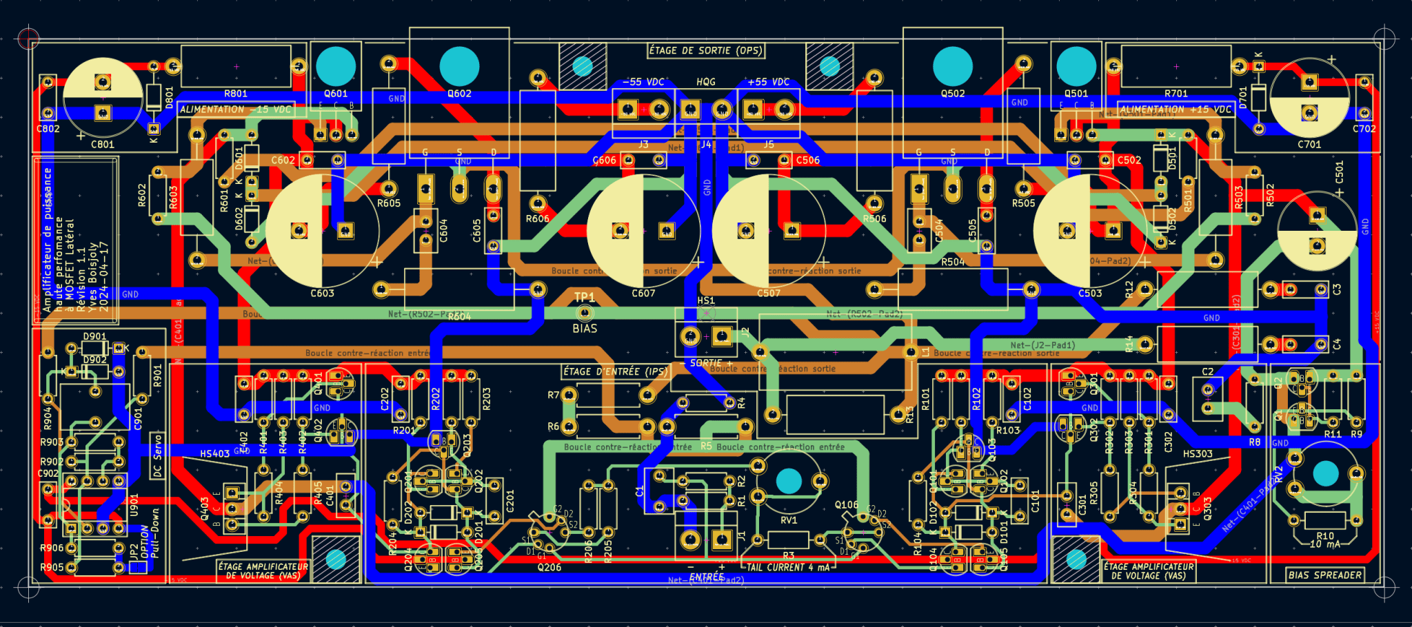
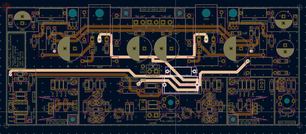
Unless I switch to a 4-layers PCB! There! Another universe emerges:
Components side (all grounds traces highlighted):
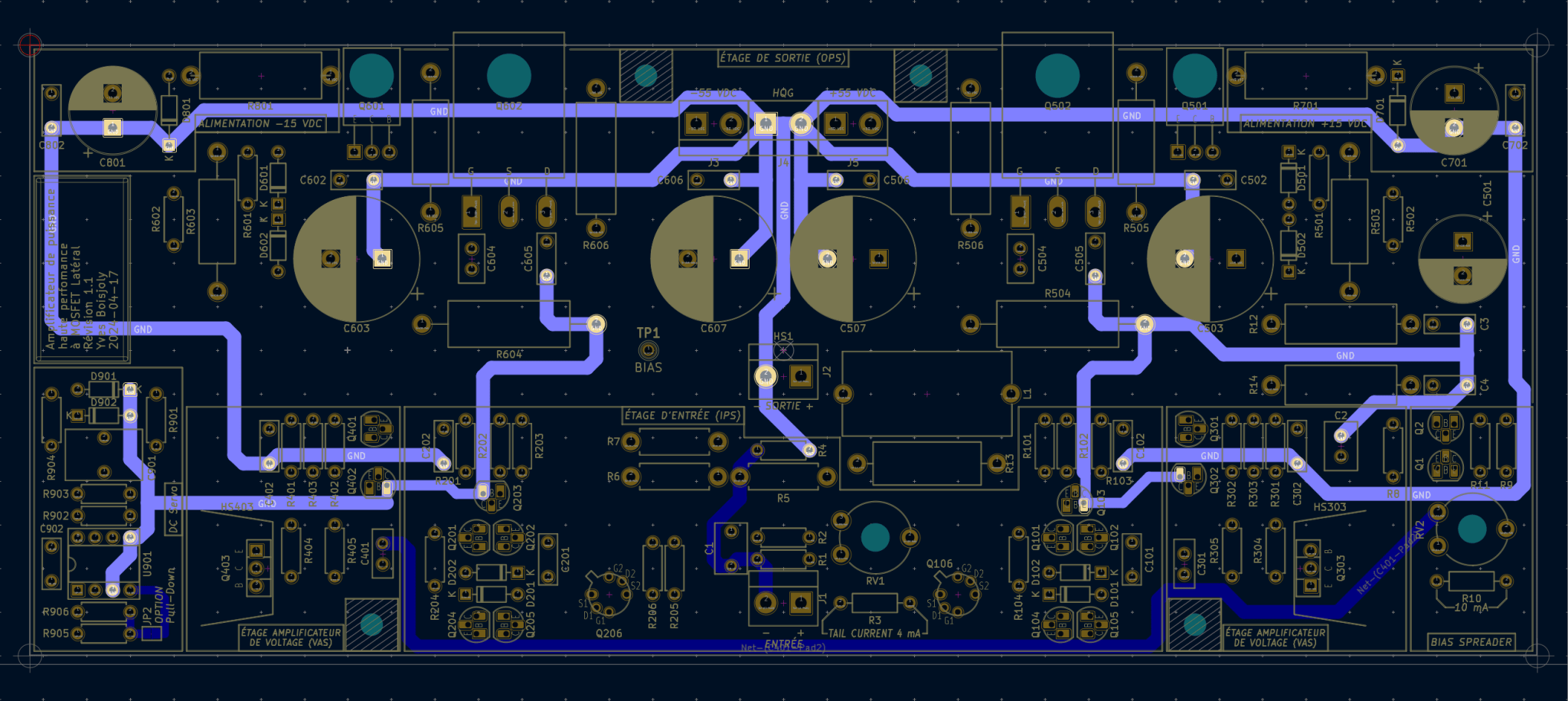
Inner copper 1 (only two ground traces):
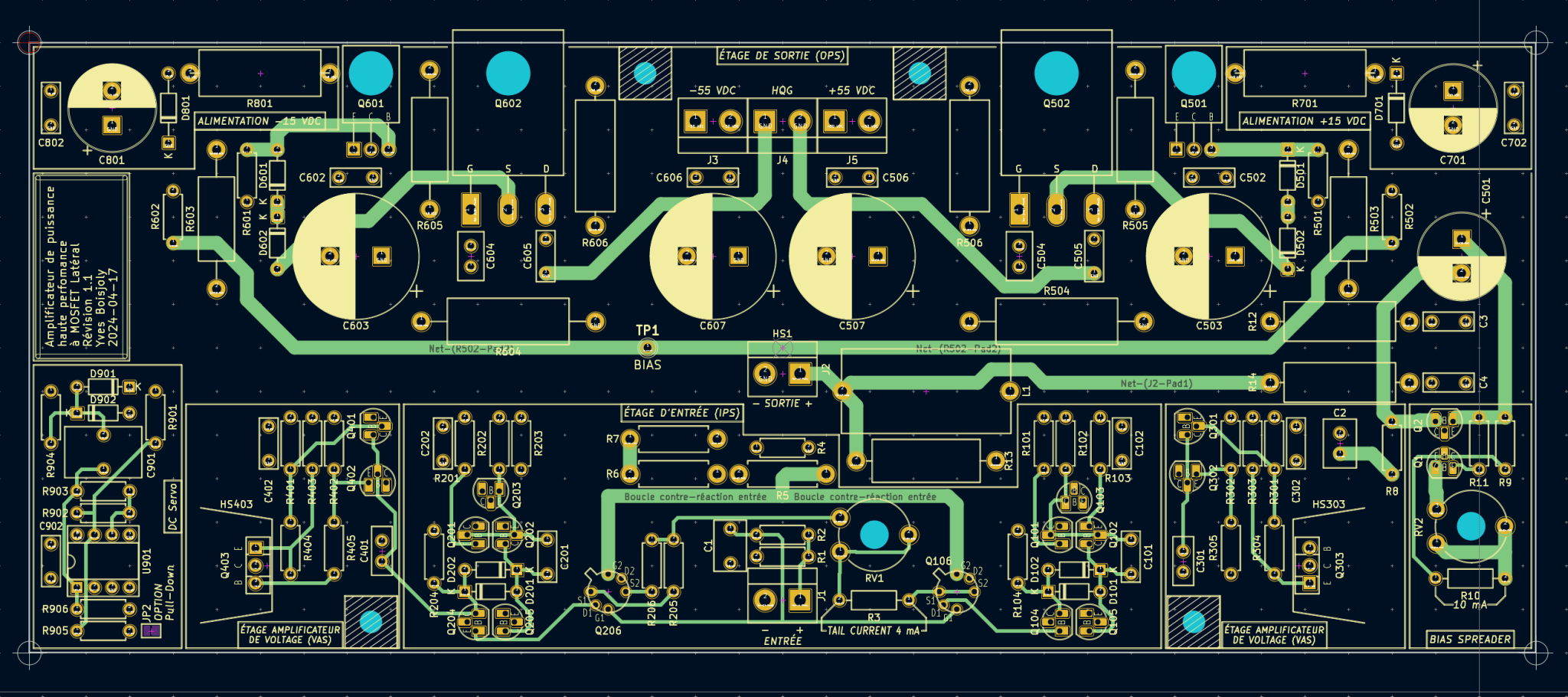
Inner copper 2:
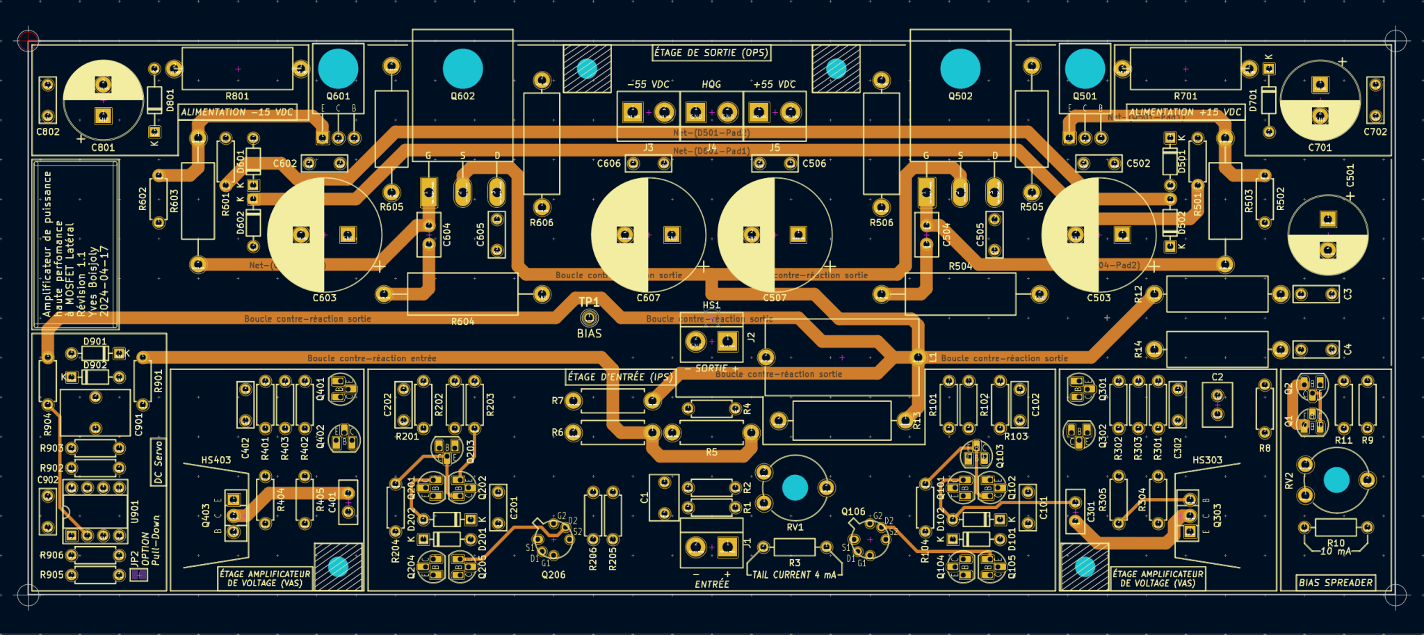
Solder side (all rails traces are on this solder side):
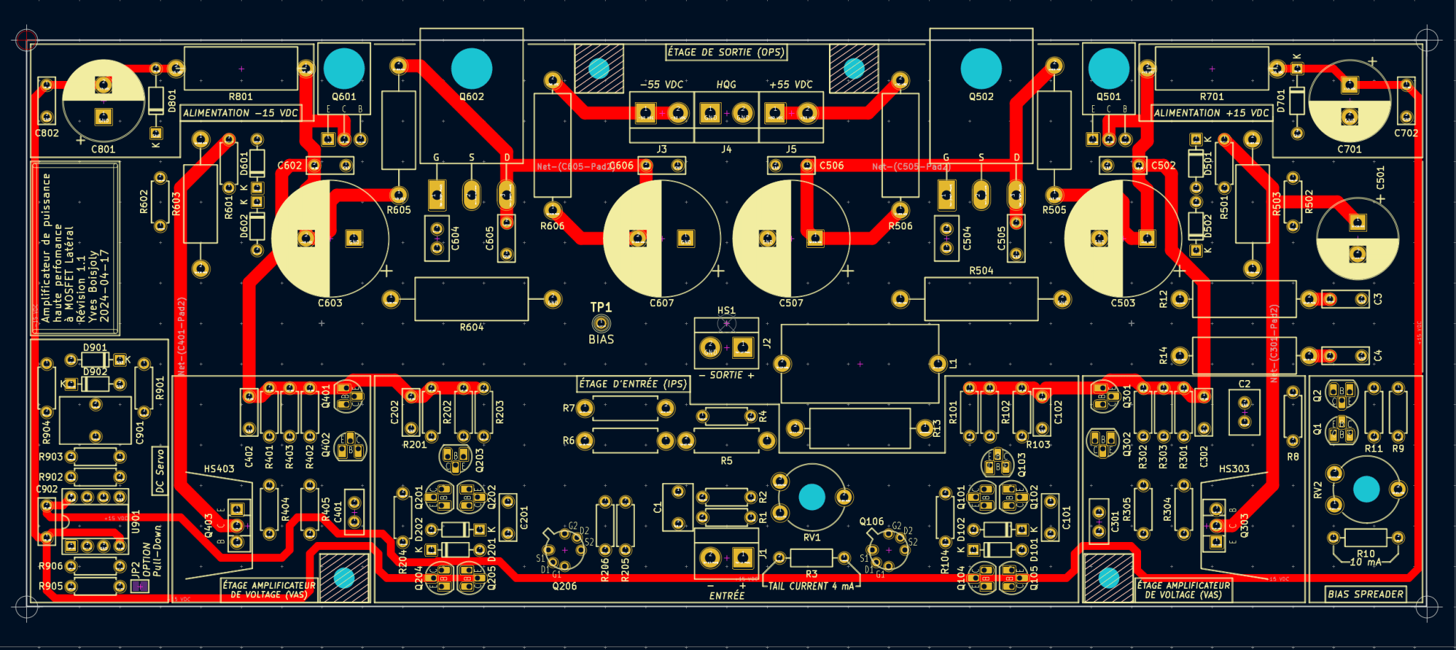
All layers on:
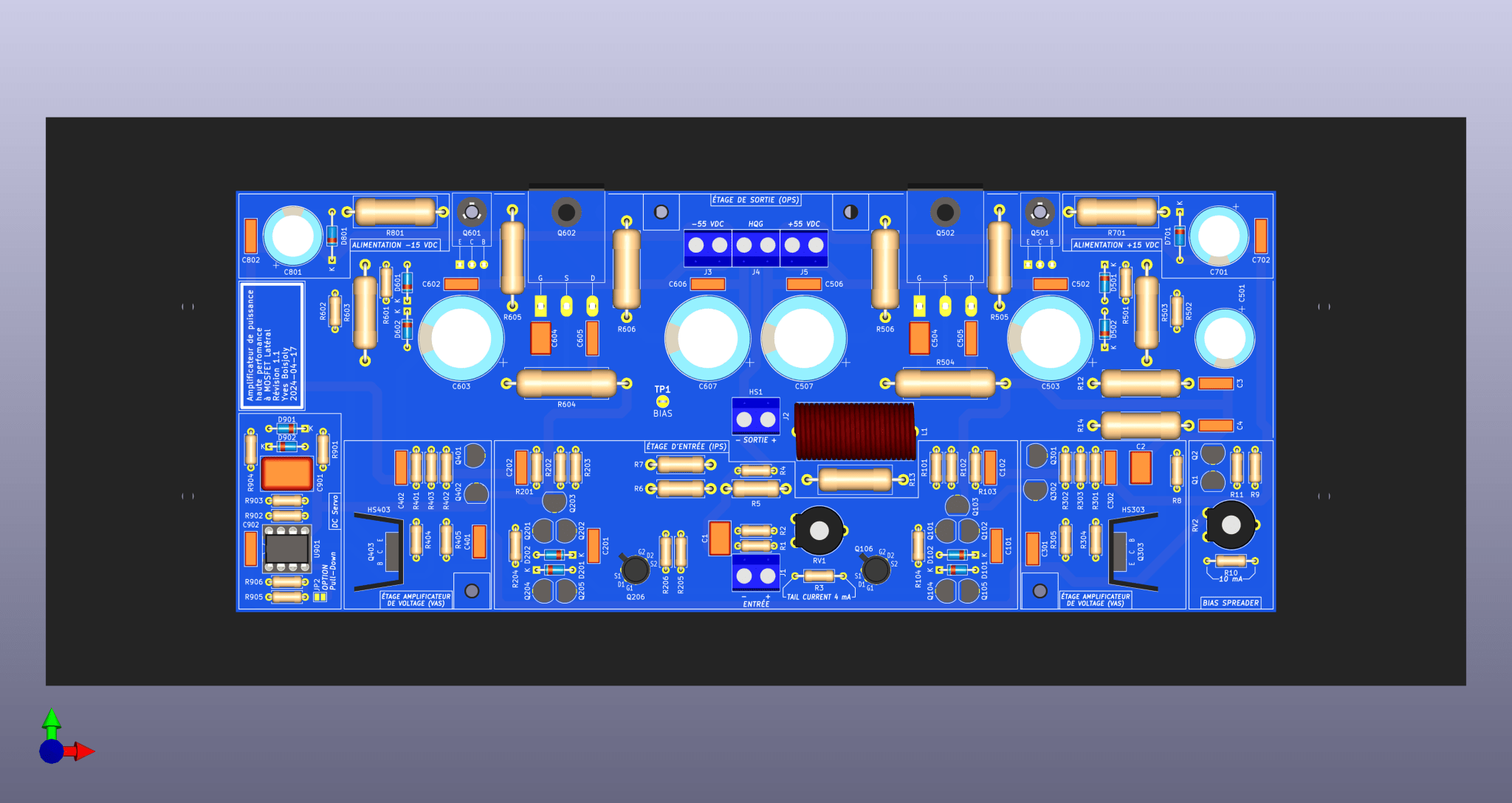
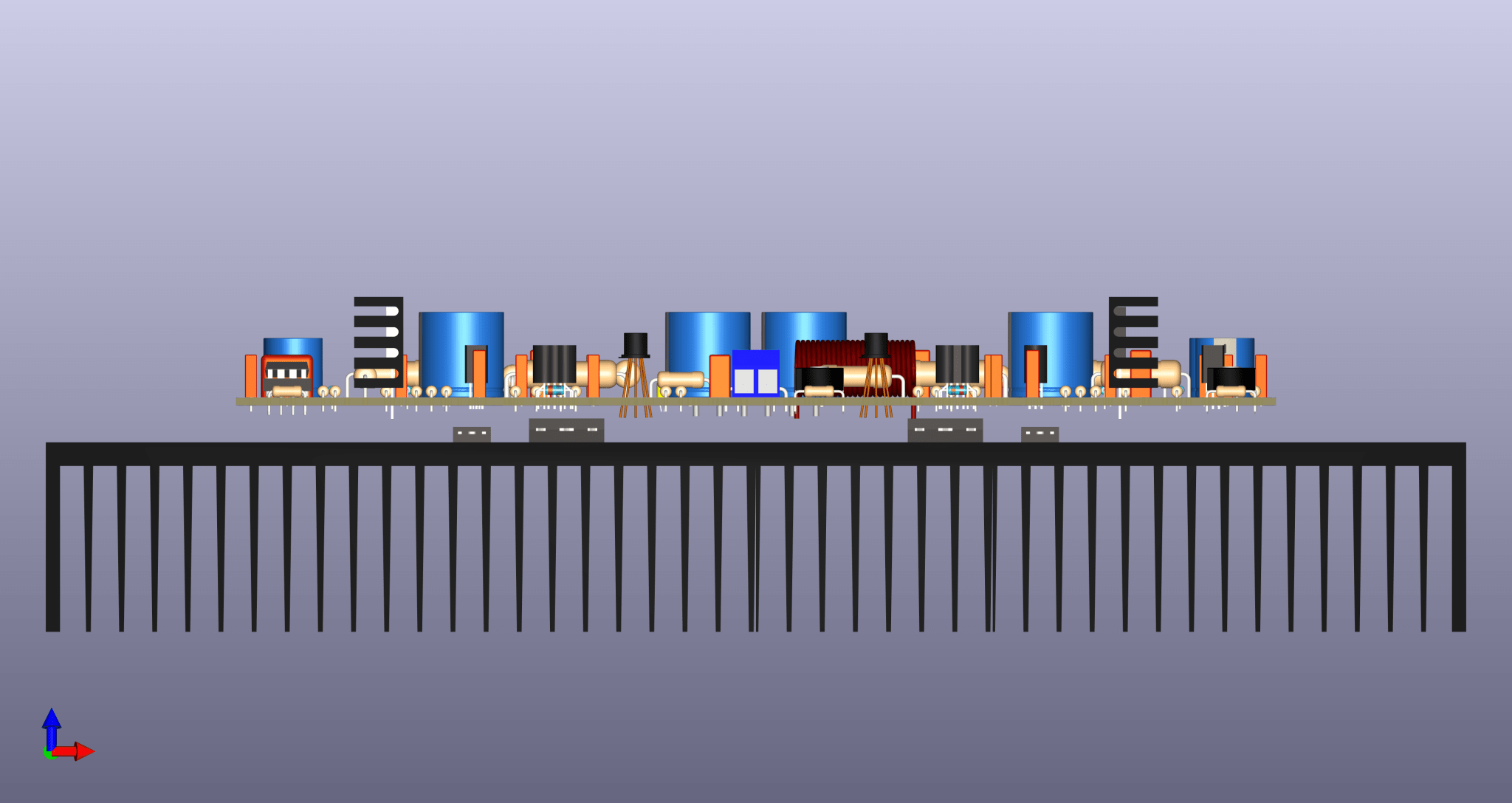
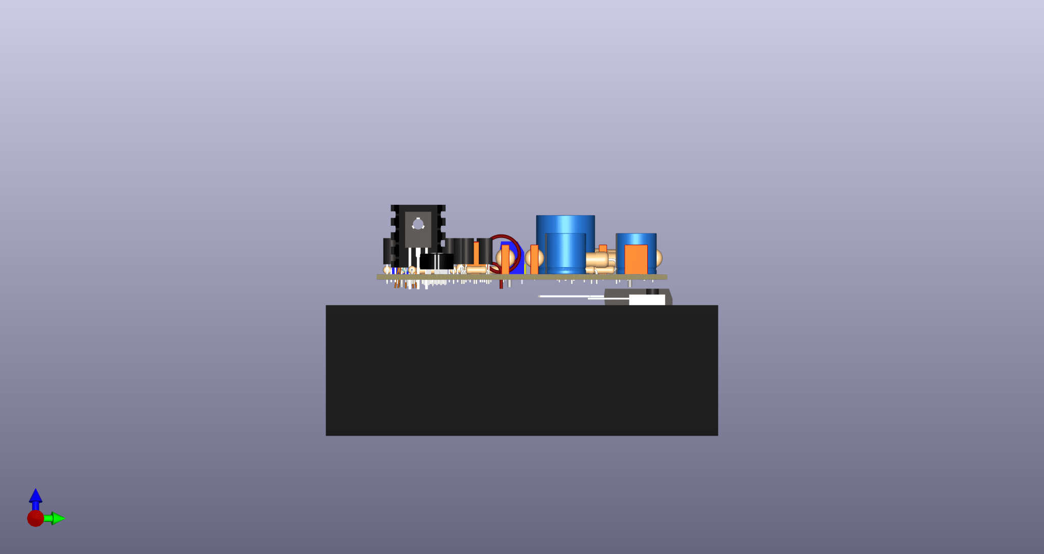
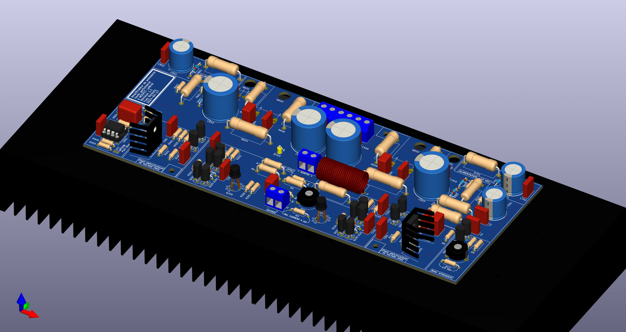
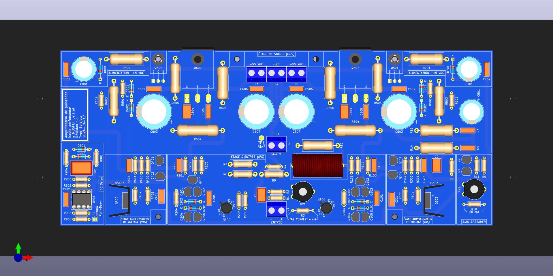
3D Views:
Unless...
Unless I switch to a 4-layers PCB! There! Another universe emerges:
- much greater latitude to limit long power supply traces
- the possibility of isolating all decoupling capacitor ground traces from those of the audio signal, while preserving a star topology
- the ability to place feedback resistors close to input and output connectors, without blocking other paths
- and more and more...
- the limited height of the 3U heat-sink
- respect for the prefabricated mounting holes according to the "diyAudio Universal PCB & Semiconductor Mounting Specification (UMS)" drawing
- power supply traces as short as possible, close to the output transistors
- ground traces between R4 resistor and input and output connectors as short as possible
- input, output and supply connectors positioned as centrally as possible, so that the circuit can be rotated from left to right for the left and right channels, preserving symmetry.
Components side (all grounds traces highlighted):
Inner copper 1 (only two ground traces):
Inner copper 2:
Solder side (all rails traces are on this solder side):
All layers on:
3D Views:
In parallel to this design, I do read back all my books for the second time. I noticed from Douglas Self book that the coil L1 should be placed as far as possible from the output transistors. So I switched the position of the coil L1 and it's parallel resistor R13 in order to move away the coil from the output transistors. That didn't modify the traces design from their restrictions.
I'm noting a couple of things as I notice them..
The zeners for +/-15V seem to be at opposite corners of the board. Same with the +/-55V lines fanning out in opposite directions. Where possible, you should apply the same logic as for "twisted pair" cabling. The wires should not have so much empty space before they encounter any shielding. I'm not talking about the minimum necessary to maintain isolation, but generally, opposite voltages should be right next to each other.
If you can't move C701 / C801 closer to the cascode bases, then maybe add a couple of small capacitors?
See post #1 where the links below are available:Post à schematics?
From the first link, go to post #139
You see, if you look carefully how the +/-rails are distributed in series into the schematic, and keep in mind that their ground return should be as close as possible to the start HQG, it is physically impossible to put all those cans in the same place, close to the +/-rails connectors, neither to keep their traces close together as well as distributing their voltages to their target parts! Trust me, I tried!The zeners for +/-15V seem to be at opposite corners of the board. Same with the +/-55V lines fanning out in opposite directions. Where possible, you should apply the same logic as for "twisted pair" cabling. The wires should not have so much empty space before they encounter any shielding. I'm not talking about the minimum necessary to maintain isolation, but generally, opposite voltages should be right next to each other.
If you can't move C701 / C801 closer to the cascode bases, then maybe add a couple of small capacitors?
The first goal is to have the output transistors symmetrically placed on the heat-sink, onto the preset holes in the heat-sink. Once that is fixed, the tiny 3.5 inches of height available on the PCB, forced by the heat-sink height, is blocking the traces distributions and at some point there are no more place to pass the traces without sacrificing a rule that should not be sacrificed!
Let's analyse the path design for example. The +/-50 VDC rails are all symmetrical. So let's follow the path of the +50 VDC. (I just realized I should update my silkscreen that says wrongly +/-55VDC!). You start at the +50VDC and reach the R506 serial resistor, as close as possible to the connector while keeping the mounting hole available to support the screw forces when the user will tighten the screws, then R506 goes to the filter capacitor C507 and C506, just before it reach the output Drain MOSFET Q502:
Taping from that point to reach the next serial resistor R505, again that continue to it's decoupling capacitor C503 and C502 before it reach the driver Q501 collector. Just from the last decoupling capacitor C502, I follow the R701 resistor to start the +15VDC as short as possible, and also to reach the VAS and IPS circuit with the shorter path I can. I already have consumed half the height available and still have to put the output coil with it's R13 resistor and the two Zobel huge resistors R12/R14 of the output!
Moving C701/C801 closer to the +/-15VDC parts is futile because the place isn't available. I admit I though to move at least the C702/802 decoupling ones closer to their parts circuit.
Then you still have to respect these:
- Closer and shorter path for the NFB traces
- L1 coil closer to the Input instead of close to the Output transistors
- With that come the R13 huge resistor in parallel
- You still have to think where you will put the BIAS SPREADER and the DC Servo
- This latest need +/- 15 VDC and ground to it's IC. How do you achive that wile keeping it close to both the NFB Input and Output as well as the +/-rails traces
As Bob Cordell says; "You have to choose your poison!" I choose to sacrifice the +/-15 VDC path.
You are right, something weird come in by copy/paste those links. Here find it below...Maybe I'm blind, but neither post #1 (int his thread) mentioned above, nor the links mentioned above, point to anything that looks like a schematic....
Attachments
I can see clearly, but the output rail, Plus rail and ground to one side must be laid on top of and next to each other. On the other side, the minus rail, output rail and grounds must be laid on top and next to each other. The rail decoupling capacitors must connect directly to the power ground tracks mentioned above. The small signal front-end ground and feedback loop must be kept to a small loop and the small signal ground taken directly back to the incoming PCB central star ground. Do not connect any decoupling capacitors or anything else to the small signal front-end ground It is very important that the above things are done to keep the loop areas small.
"After more than fifteen attempts, moving parts around in turn in order to respect all the advice I'd gathered, I've come to the conclusion that this schematic circuit is not feasible in a space limited by the 3U heat-sink..."
Just keep working at it until you get it right. Better to spend an extra few weeks ripping up tracks and re-routing than rushing to board fabrication and ending up with a suboptimal result.
How much current do the cascode transistors draw? At a guess, you could increase R701 / R801 by a factor of 10, if not more. If you need a very stable base voltage, you could use a shunt regulator in place of the zener, but you may be able to get away with a 36k + 15k resistor divider. 0.25W resistors running comfortably within their power ratings.
Also, electrolytics tend to have high leakage if they are run significantly below their rated voltage. 16-25V should be safe (for the 15V supply).
Also, electrolytics tend to have high leakage if they are run significantly below their rated voltage. 16-25V should be safe (for the 15V supply).
Last edited:
This schematic is the original "Figure 9.20 Example of IPS-VAS" and "Figure 14.17 A High-Performance Lateral MOSFET Power Amplifier" from Bob Cordell book "Designing Audio Power Amplifiers - Second Edition". The +/-15 VDC rails with Zener and the DC Servo circuit are taken from it's "Figure 11.19 A Vertical MOSFET TMC Amplifier" from the same book.How much current do the cascode transistors draw? At a guess, you could increase R701 / R801 by a factor of 10, if not more. If you need a very stable base voltage, you could use a shunt regulator in place of the zener, but you may be able to get away with a 36k + 15k resistor divider. 0.25W resistors running comfortably within their power ratings.
Also, electrolytics tend to have high leakage if they are run significantly below their rated voltage. 16-25V should be safe.
I never risked to change anything except for the Output MOSFET and Driver transistor number. I took care to draw the original circuit in LTSpice and compared all the simulations with the MOSFET and Driver replaced.
Not that I am aware of...In that case, is there a reference PCB layout?
@Bonsai,
This is the only way I could imagine having the +50 VDC close to the -50 VDC back to the Output MOSFET, as well as the +49 VDC/-49 VDC (After the loss in R506/606) reaching the Drivers... Am I starting the right way? It seems weird to me to voluntary route +/- rails longer just to have them as close as possible along their path.
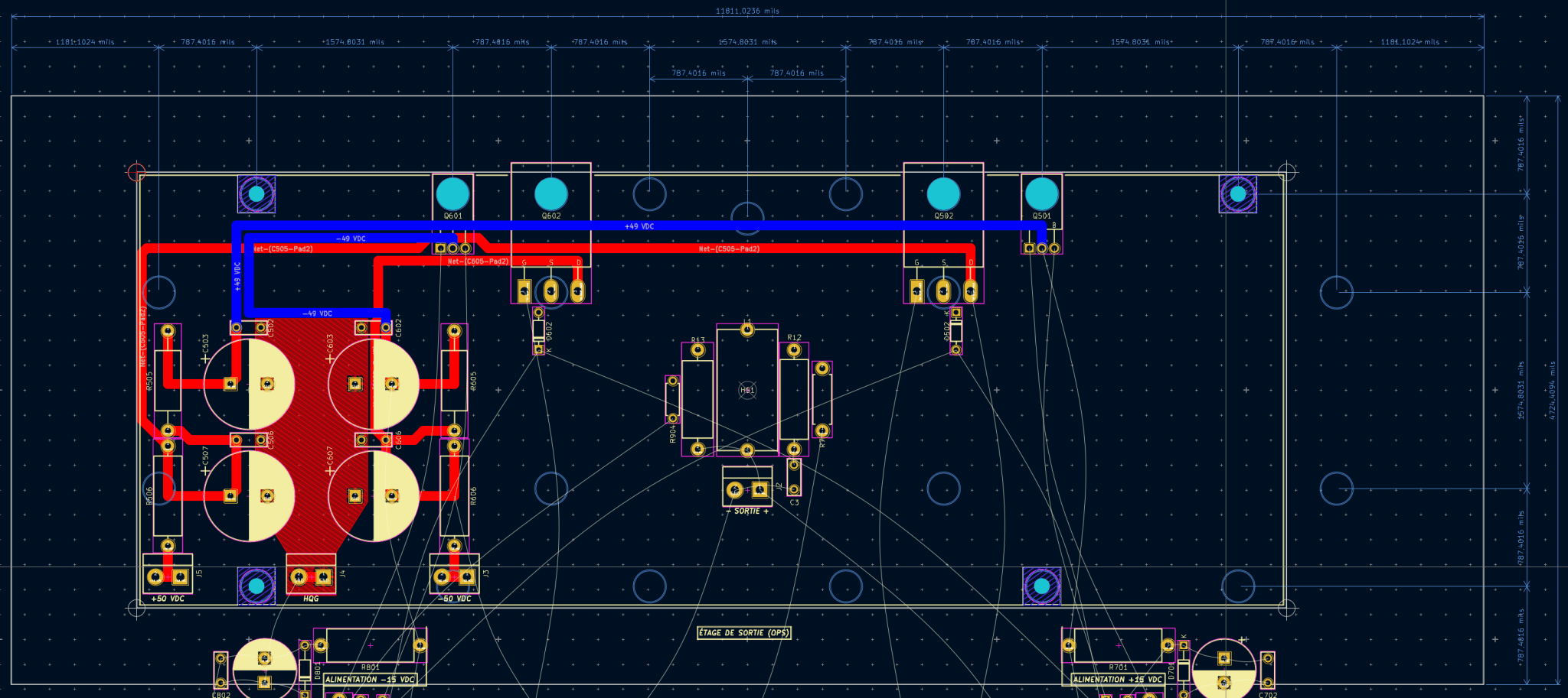
This is the only way I could imagine having the +50 VDC close to the -50 VDC back to the Output MOSFET, as well as the +49 VDC/-49 VDC (After the loss in R506/606) reaching the Drivers... Am I starting the right way? It seems weird to me to voluntary route +/- rails longer just to have them as close as possible along their path.
This is looking better. In an amp, ideally you want the power and speaker output + speaker return to all be bunched closely together - so move your output coil over to the left. Keep your input stage over to the right. Don't worry about the slightly longer traces - the loop area reduction brings serious benefits for noise. For the driver dropper resistors (R505 and R506), why don't you move those and the associated caps closer to the drivers - just tap off the supply rail, and then return the filter cap ground side to the ground track you are going to run along with the plus, minus and speaker output rail? Note for your small signal front-end signal ground, you must take that off right at the HQG connector - do not be tempted to take it from the top side near C502/C602
Don't get caught out by the 'shorter is better' idea - in many cases, it is not. Loop area is more important other than for very high current tracks - but you can always compensate for that with thicker tracks and or adding a piece of copper wire you solder along the bottom of the board (clear the solder mask for this when you do your final tweaking just before ordering your board).
Don't get caught out by the 'shorter is better' idea - in many cases, it is not. Loop area is more important other than for very high current tracks - but you can always compensate for that with thicker tracks and or adding a piece of copper wire you solder along the bottom of the board (clear the solder mask for this when you do your final tweaking just before ordering your board).
Last edited:
- Home
- Amplifiers
- Solid State
- A Lateral MOSFET Power Amplifier Design Version 1.1