Hello fellow DIYers !
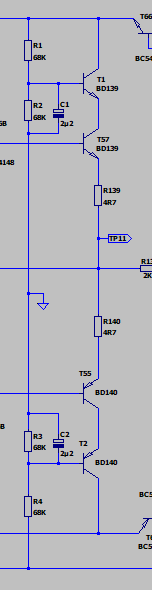
With much help from the fine folks here I begin to master the design intricacies of my vintage integrated amp's MM/MC phono stage. The amp is 30+ years old and the only schematics I could find online were for the revision 3 of the design, whereas my unit is rev. 1. When trying to match the PCB to the schematic there were areas I couldn't make heads or tails, and it turns out there's a major difference on the implementation of the output stages.
Rev 1 implements a cascode stage while Rev. 3 doesn't; of course in both cases the output (TP13) is still taken off the center of the push-pull stage. See below.
Rev 1:

Rev. 3:

So my question is, why use a cascode at all if the output is not taken off the top transistor's collector? The top collectors are directly connected to the supply so there can't be any output taken there. My guess is to mitigate power dissipation in the output devices since the supply voltages are relatively high (The phono stage shares the same regulated voltage as the power amp section). But if it is for this reason, why drop it in Rev. 3, since that version has the same supply voltages? Simply to save a few transistors I guess... Or are there other advantages I don't understand? A cascode provides extra input to output isolation, but only if the output is taken off the top collector right?
Note that the second stage's output has the same cascode arrangement but with extra filtering capacitors between ground and base of the top transistors :
Thanks in advance for any insights, and let me wish you all the best for 2024, good health and successful projects!
- Joris
With much help from the fine folks here I begin to master the design intricacies of my vintage integrated amp's MM/MC phono stage. The amp is 30+ years old and the only schematics I could find online were for the revision 3 of the design, whereas my unit is rev. 1. When trying to match the PCB to the schematic there were areas I couldn't make heads or tails, and it turns out there's a major difference on the implementation of the output stages.
Rev 1 implements a cascode stage while Rev. 3 doesn't; of course in both cases the output (TP13) is still taken off the center of the push-pull stage. See below.
Rev 1:
Rev. 3:
So my question is, why use a cascode at all if the output is not taken off the top transistor's collector? The top collectors are directly connected to the supply so there can't be any output taken there. My guess is to mitigate power dissipation in the output devices since the supply voltages are relatively high (The phono stage shares the same regulated voltage as the power amp section). But if it is for this reason, why drop it in Rev. 3, since that version has the same supply voltages? Simply to save a few transistors I guess... Or are there other advantages I don't understand? A cascode provides extra input to output isolation, but only if the output is taken off the top collector right?
Note that the second stage's output has the same cascode arrangement but with extra filtering capacitors between ground and base of the top transistors :
Thanks in advance for any insights, and let me wish you all the best for 2024, good health and successful projects!
- Joris
Attachments

Does it limit output swing perhaps? Is it really a cascode - we can't see enough of the circuit to be sure...
Actually it's not a cascode because the output is not taken from collector of the top transistor. Rather it's a voltage regulator that provides a halved voltage supply for output transistors. This reduces the available swing and overload margine, but I bet there is still plenty left.
Possible reasons for such solution is:
Possible reasons for such solution is:
- need to reduce max voltage seen by output tranzistors
- to reduce dissipation
- to further decouple supply of previous stages from demanding output stage
Thank you for your replies. Here is the full schematic but it's kind of large - If needed I can supply the relevant LTspice files. You're right, it may rather be a voltage regulator than a cascode. The power supply rails are +-40v so well within the specs of the BDs and the current is low, but decoupling of output stage from the previous sensitive input gain stages makes sense. Of course halving Pdiss is a good thing too, without the regulator Pdiss was a high-ish 580mW per transistor.
I am cloning this design as a DIY build and thinking about incorporating the first stage's regulators. The reduction in Pdiss is not an issue in my version since it is modified to run on +-15V rails but if it helps in the sonics department it may be worth while. However due to JLCPCB board size limitations I don't think I can integrate the last stage regulators with their bias networks...

I am cloning this design as a DIY build and thinking about incorporating the first stage's regulators. The reduction in Pdiss is not an issue in my version since it is modified to run on +-15V rails but if it helps in the sonics department it may be worth while. However due to JLCPCB board size limitations I don't think I can integrate the last stage regulators with their bias networks...