Hello, hope everyone is having a great weekend 
I'm designing a shunt regulator which is fed by a high-side CCS. My previous design uses a 5.6V zener as the reference for the pass mosfet; This works but current regulation is not so good due to zener noise. Also the zener needs a minimum of 5 mA current to control noise so there is power wastage in the feed resistor to the zener. Moreover this zener current bypasses the CCS and has to be regulated downstream by the shunt mosfet.
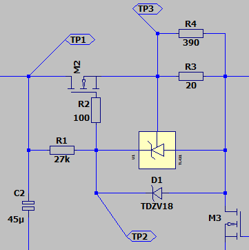
I redesigned the circuit as a text-book TL431 current source with the difference that it is floating at HV (partial schematic of the relevant section below). In simulation the current regulation is really good, within a milliamp, and the TL431 only need a milliamp to regulate - The design is so that the minimum current through it is around 1.2 mA, and peaks at 2.2 mA. This represents a very significant power wastage reduction in feed resistor R1.

At start-up when the output capacitor (not shown) isn't charged the device will see the full rectified voltage from the 45 uF input capacitor across its anode and cathode (350v peaks). To protect it and the mosfet gate there's a 18V zener that will get out of circuit when the TL431's AK voltage differential drops below the zener threshold - so it won't contribute noise in normal operation. I have seen this TL431 protection scheme in other circuits online but they were all "low-side", e.g. the TL431 anode was grounded. Will it work in my proposed circuit?
Also I read that the TL431 likes to oscillate when driving an external transistor. Some suggest a compensation capacitor between cathode and reference. Is it a good idea in the context of this circuit? I would think such a capacitor can mess with M2's gate/source capacitance and create more problems than it solves.
Lastly, are there no-no's I don't see with my beginner eyes?
As always, thanks in advance for any insights.
- Joris
I'm designing a shunt regulator which is fed by a high-side CCS. My previous design uses a 5.6V zener as the reference for the pass mosfet; This works but current regulation is not so good due to zener noise. Also the zener needs a minimum of 5 mA current to control noise so there is power wastage in the feed resistor to the zener. Moreover this zener current bypasses the CCS and has to be regulated downstream by the shunt mosfet.
I redesigned the circuit as a text-book TL431 current source with the difference that it is floating at HV (partial schematic of the relevant section below). In simulation the current regulation is really good, within a milliamp, and the TL431 only need a milliamp to regulate - The design is so that the minimum current through it is around 1.2 mA, and peaks at 2.2 mA. This represents a very significant power wastage reduction in feed resistor R1.
At start-up when the output capacitor (not shown) isn't charged the device will see the full rectified voltage from the 45 uF input capacitor across its anode and cathode (350v peaks). To protect it and the mosfet gate there's a 18V zener that will get out of circuit when the TL431's AK voltage differential drops below the zener threshold - so it won't contribute noise in normal operation. I have seen this TL431 protection scheme in other circuits online but they were all "low-side", e.g. the TL431 anode was grounded. Will it work in my proposed circuit?
Also I read that the TL431 likes to oscillate when driving an external transistor. Some suggest a compensation capacitor between cathode and reference. Is it a good idea in the context of this circuit? I would think such a capacitor can mess with M2's gate/source capacitance and create more problems than it solves.
Lastly, are there no-no's I don't see with my beginner eyes?
As always, thanks in advance for any insights.
- Joris
I can't think of any reason why the protection wouldn't work, but I also don't understand why the full voltage is across the TL431 at start up without protection. Shouldn't most of the voltage drop across R1? Or is the current required for that more than the TL431 can handle?
TL431 is a bandgap reference, and those are usually not very low noise either. I vaguely remember that TL431 is a relatively good one, though.
TL431 is a bandgap reference, and those are usually not very low noise either. I vaguely remember that TL431 is a relatively good one, though.
why the full voltage is across the TL431 at start up without protection
Thanks Marcel for your reply. I took this notion from one of my books. Describing the error amplifier transistor in the following circuit :
[sic] "When working, the error transistor only has VCE = 88 V, but at the instant of start-up, the 22 mF Zener bypass capacitor clamps the emitter of the error amplifier to 0 V, so it must be able to survive VCE = 330 V."
I believe the same phenomenon applies to my circuit. You are an expert and I trust your advice, so there is either something wrong with the statement or I misunderstood it. I can be thick at times!
The way I understand it, say by bad luck the mains is at its peak when switching on my circuit, the input capacitor receives a strong inrush current and its voltage raises quickly; the output capacitor is at ground. Current begins to flow through R1 and the output voltage will raise quickly as well reducing the differential across the TL431, but at the very beginning there is little current flow hence little voltage drop across R1 so there is a moment where the maximum voltage across the TL431 is exceeded.
With the zener in place, the TL431 sees only the 18V Vz and "floats" at the input voltage minus the drop across R1 while the bulk of the voltage is applied to the output capacitor, until it is charged enough that the voltage across the zener is below its Vz and the TL431 is operating in its normal design conditions.
Of course implementing zero-crossing switching and inrush current limiting might mitigate this condition but I rather design for the worst-case scenario.
Last edited:
Also I read that the TL431 likes to oscillate when driving an external transistor. Some suggest a compensation capacitor between cathode and reference. Is it a good idea in the context of this circuit? I would think such a capacitor can mess with M2's gate/source capacitance and create more problems than it solves.
First idea that comes to mind is to put some capacitor between anode and cathode of U1 (10nF perhaps). It could increase stability and provide additional protection from transient overvoltage. The downside is slightly reduced regulation at high frequencies, but it shouldn't be a problem.
10nF (or 1nF for that matter) produces a metric ton of ringing in simulationput some capacitor between anode and cathode of U1 (10nF perhaps).
I'm not sure if that capacitor is needed or desirable, but assuming it is:
Calling the ringing frequency fr and the capacitance C, you could try connecting a resistor with a resistance close to R = 1/(√2 π fr C) in series with the capacitor. The closest E12 value should do. This creates a zero in the loop gain that should damp the ringing, or so I hope.
Calling the ringing frequency fr and the capacitance C, you could try connecting a resistor with a resistance close to R = 1/(√2 π fr C) in series with the capacitor. The closest E12 value should do. This creates a zero in the loop gain that should damp the ringing, or so I hope.
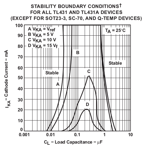
Digging in the TL431 datasheet I found the stability boundary conditions graph (see below). The relevant conditions for my circuit are the "B" curves. I'm operating the TL431 at 2-5mA and the pass mosfet has a high-ish input capacitance between 2.2-2.8 nF. In these conditions the TL431 may become instable with as low as 9nF capacitance. I have not yet tested the snubber arrangement suggested by Marcel as I'm not sure of the advantages of having a capacitor acros AK...

- Home
- Amplifiers
- Power Supplies
- Protecting TL431 in a high voltage high-side current source