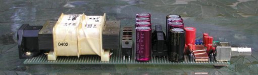
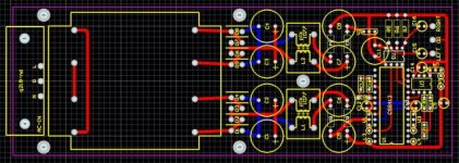
48V Hammond transformer provides double secondaries (12V ea.), full bridge rectifiers consist of MSR860. After that there is a first capacitors bank, followed by common mode chockes, more caps, series resistors, and finally BG caps at the of the filtering chain. All local bypasses consist of BG N, all regulators are AN800x.
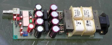
It still doesn't show, but output RCAs will be also PCB mounted. Nice thing about that layout is that it fits inside 3 x 2 aluminum tubing, so chassis construction will be simplified (it's hard to predict how it will sound though)")
It still doesn't show, but output RCAs will be also PCB mounted. Nice thing about that layout is that it fits inside 3 x 2 aluminum tubing, so chassis construction will be simplified (it's hard to predict how it will sound though)
Attachments
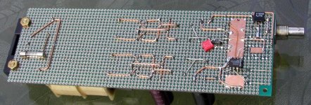
Don't let the lack of PCB to stopp your desire to produce top notch circuit. I believe that this is almost as good (or even better) than a PCB TDA1543 is on the bottom side to simplify the I2S connection (the tree wires in the air).
Also, using copper groundplanes doesn't have to look dead bug style and messy.
TDA1543 is on the bottom side to simplify the I2S connection (the tree wires in the air).Also, using copper groundplanes doesn't have to look dead bug style and messy.
Attachments
Peter Daniel said:Don't let the lack of PCB to stopp your desire to produce top notch circuit. I believe that this is almost as good (or even better) than a PCB
A pcb would make it easier to build though...
(layout almost finished, once the ground plane and BNC jack is added)
--
Brian
Attachments
Bricolo said:What's the difference between the green and the brown veroboards? (except that the first cost the double)
It seems like green ones are made of better material. Also, the pads are gold plated (and holes are through plated and smaller), I'm using them only for special projects
I checked again, with this DAC, the influence of ceramic bypass caps. I've built the DAC without those caps initially and listened to it after 24hours warming period. The sound seemed dry and missing sparkle.
Later, I added my usual ceramic combo (0.015 @ 0.33), and both presence and dimentionality improved (as well surprisingly, the bass response). I don't have any doubts that those caps are an improvement.
Later, I added my usual ceramic combo (0.015 @ 0.33), and both presence and dimentionality improved (as well surprisingly, the bass response). I don't have any doubts that those caps are an improvement.
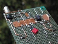
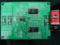
this is test print, any recommend was welcome. I still can improve.
Wow...real pretty board...
Good work Thomas.
Regards,
Bas
Peter, nice work! I have been contemplating the photos over the weekend.
Some questions:
1.) What are those things connected to the AN800X regulator legs? They are marked on your 2-D schematic with circles, and two are connected in series to Vin of each reg, I think.
2A.) Why did you mount one ceramic cap chips for bypass on the bottom of the test board, and not for shortest signal pass directly on the chip pins of the CS8412 (7 and 8, for dig supply, and 22 and 21 for analog supply), since V+ and GND are conveniently next to another on CS8412? Are the chip caps you use too large for this, and thus pcb SM pads required?
2B.) Related question: is the second supply bypass chip cap then mounted directly between the reg pin and the copper foil ground plane above the CS 8412? Which bypass cap is above, and which below?
3.) Why do you connect serial port mode select 1 (M1, pin 24) to VD+ and not VA+?
4.) Why did you choose 470R/220n for PLL, and not stock 1k/.047uF?
5.) I see you used the wildmonkeysect 3n3 bypass on the PLL--any impressions?
6.) Where can one see a schematic of your choke-regulated supplies?
Best regards,
James
Frankfurt
- Status
- This old topic is closed. If you want to reopen this topic, contact a moderator using the "Report Post" button.
- Home
- Source & Line
- Digital Source
- The ultimate TDA1543 DAC layout??