However, for a current mirror to track well a small resistor should be inserted in the emitters, typically 68R.
R
R
I see, I am out hereJ113 will typical see less than half of 40V.
R
Last edited:
Just a quick analysis of mine just by gleaning over the schematic, so it may be incorrect, but here it goes.. At power up c4 is discharged which forces ltp u4 to become virtually grounded, its emitter voltage will not stand much above ground and therefore could initially cause the ccs to be exposed to near full rails voltage, and if the chosen transistor in the CC's can't withstand the voltage seen over it there is a risk it could break down. To some degree u3 and c1 could potentially cause a similar problem, but would depend on the pulldown current through current mirror u7 which depends on u8 biasing current.
Solution is to choose a ccs transistor that can withstand on its own the required voltage, or cascode it with a transistor that can handle it, or put a resistor in series with ccs to drop down the voltage, say 10-15 volts.
10v / 5.5mA is about 1,8k ohm.
For simplicity and philosophy of this amplifier I think I would go with the series resistor. :)
Yes, that’s sound engineering I agree with (using the same solution in my build). However, Nelson confirms that J113 is safe up to 50V. 🙂or put a resistor in series with ccs to drop down the voltage, say 10-15 volts.
https://www.diyaudio.com/community/threads/diy-front-end-2022.394339/post-7235215
More important might be what's missing. Overload behavior / proper clipping, how the operating point is reached (audible effects), behavior with capacitive loads, temperature stability. The issue with jfet Vds(max) could have been avoided by using RF types (like BF245,246, 247): they're designed with resonant LC in the drain so can handle the "extra" AC. With this in mind, the next issue is to verify that the sim provides data in accordance with the manufacturer's specs. I always verify Hfe of the bjts is in accordance with what I read from actual measurement of the device. Measuring every component that enters a circuit under construction has been a guarantee that it behaves as in the sim.
Yes, the change is simple. Another improvement would be to split R9 into 2 Rs and adding a C from the common node to ground. That increases the gain in a way that less compensation is required, improving the slew rate while keeping the overal frequency response flat. The use of mosfets allows inclusion in the compensation network without causing instability at overload so also decreases distortion.
before diving into a PCB attempt I did a LTspice simulation.
I swapped KSA1381 and KSC3503 for BD140C and 139C, because 80 V Vceo should be enough.
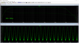
with C6 = 100 p I get a ~10 MHz oscillation:
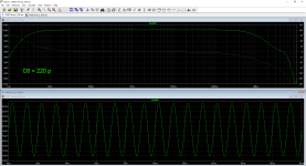
increasing C6 to 220 p removes the oscillation:
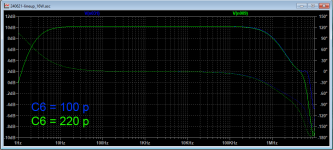
edit - here is a comparison graph:
attached is the LTspice circuit with necessary models in the ZIP. just in case anyone wants to test it or if my circuit needs to be corrected!
latefets by IanH & keantoken, BC/BDs by cordell.
I swapped KSA1381 and KSC3503 for BD140C and 139C, because 80 V Vceo should be enough.
with C6 = 100 p I get a ~10 MHz oscillation:

increasing C6 to 220 p removes the oscillation:

edit - here is a comparison graph:

attached is the LTspice circuit with necessary models in the ZIP. just in case anyone wants to test it or if my circuit needs to be corrected!
latefets by IanH & keantoken, BC/BDs by cordell.
Attachments
Last edited:
- Home
- Amplifiers
- Solid State
- 16 Watt small Amplifier with Exicon output and TMC