Are those measurements with the preamp connected to the amp?
The R1, R3, and R4 voltages are disturbing.
There should be no DC voltage across R1, which is in series with the signal input.
The voltages across R3 and R4, which are a measure of the current though the JFETs, are much too high and could damage the JFETs. Assuming that your measurements were taken with the preamp in place, did you measure the voltage across R3 and R4 when you were setting up the channel and biasing it?
Disconnect the preamp and measure the preamp output for DC offset. Set your meter to VDC and place a probe on the positive of the RCA output and the other probe on the negative of the RCA output.
Do not connect that preamp back to your amplifier.
Remeasure amplifier R3 and R4 with no preamp connected if previous measurements were made with preamp connected.
Are those measurements with the preamp connected to the amp?
The R1, R3, and R4 voltages are disturbing.
There should be no DC voltage across R1, which is in series with the signal input.
The voltages across R3 and R4, which are a measure of the current though the JFETs, are much too high and could damage the JFETs. Assuming that your measurements were taken with the preamp in place, did you measure the voltage across R3 and R4 when you were setting up the channel and biasing it?
Disconnect the preamp and measure the preamp output for DC offset. Set your meter to VDC and place a probe on the positive of the RCA output and the other probe on the negative of the RCA output.
Do not connect that preamp back to your amplifier.
Remeasure amplifier R3 and R4 with no preamp connected if previous measurements were made with preamp connected.
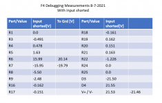
The measurements in #2797 are attached to preamp with signal.
I measured the preamp output at VDC = 0.00
I disconnected the preamp and measured R3 & R4
R3 = -0.474
R4 = 0.470
Well, you amp measures differently with preamp connected and disconnected, and it shouldn't.
With the preamp disconnected it measures better except the current through R3 and R4 is high. Where did you buy the new JFETs? They seem to be of a different grade with much higher Idss. You measured 0.47V (21mA) when 0.11V (5mA) is expected.
Short the input (connect input positive to input ground) and measure voltage across R3 and R4. There should be no change.
What is your preamp? Is it AC coupled (capacitor in series with the signal output)? Do you have another preamp?
Ben,
Where did you buy the new JFETs?
From the DIY store. Using the PEAK DCA75 Pro I show these IDSS readings:
N Idss = 6.56mA Vds = 3.01V
P Idss = 6.92mA Vds = 2.47V
Short the input (connect input positive to input ground) and measure voltage across R3 and R4.
I shorted the input and got these readings:
R3 -0.469
R4 0.468
What is your preamp?
I have been using my Akitika PR-102 Preamp thru the building of my now 4 Pass amps.
Is it AC coupled (capacitor in series with the signal output)?
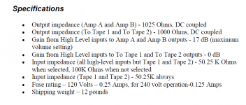
Specs [attached] are a 1025 Ohms, DC Coupled output
Do you have another preamp?
I have the Starving Student headphone amp i recently built. I used it in a test a few days ago in lieu of the PR-102.
Thanks
Where did you buy the new JFETs?
From the DIY store. Using the PEAK DCA75 Pro I show these IDSS readings:
N Idss = 6.56mA Vds = 3.01V
P Idss = 6.92mA Vds = 2.47V
Short the input (connect input positive to input ground) and measure voltage across R3 and R4.
I shorted the input and got these readings:
R3 -0.469
R4 0.468
What is your preamp?
I have been using my Akitika PR-102 Preamp thru the building of my now 4 Pass amps.
Is it AC coupled (capacitor in series with the signal output)?
Specs [attached] are a 1025 Ohms, DC Coupled output
Do you have another preamp?
I have the Starving Student headphone amp i recently built. I used it in a test a few days ago in lieu of the PR-102.
Thanks
Attachments
I don't have any experience with the tester that you have so I don't know its accuracy or how it relates to Vds of about 18V. But the voltage across R3 and R4 of 0.468V and 0.469V mean 21mA of current which is much higher than 5mA.
If 21mA is passing through the JFETs it must be coming from somewhere. Your previous measurements of voltage drops across R5, R6, R7, and R22 all show 1.6mA flowing through them from the V+ and V- supplies. 1.6mA through R6 and R7 is correct, but much more current should be flowing through R5 and R22 as it should be the sum of the current to the bias circuit and the current through the JFETs. If the numbers are to be believed, they show that the V+ and V- supplies are not supplying any current to the JFETs, yet R3 and R4 voltages indicate there is current through them. The numbers are not adding up.
To confirm that, please measure the voltage drops across R5, R6, R7, and R22. And across R1, for good measure. And across R3 and R4 again.
Your preamp is DC coupled so it can pass DC. The Starving Student is AC coupled, with a capacitor at its output, so it cannot pass DC. You said you tested with it a few days ago. More information please. What was the result? Was that with the new JFETs installed?
The output stage seems to be working properly as indicated by your measurements so it is the front end that is behaving strangely.
Check your wiring again - from power supply to board and from board to input and out jacks, make sure that there are no wires from the back of the circuit board touching the heat sink, and check the V+ and V- voltages at the board.
"To confirm that, please measure the voltage drops across R5, R6, R7, and R22. And across R1, for good measure. And across R3 and R4 again."
Take these measurements with no hookup to Preamp correct? and with input shorted?
I don't understand the impact of a preamp that is DC coupled vs. AC?
I will rerun measurements with the student amp. I used it previously before the current JFets.
Take these measurements with no hookup to Preamp correct? and with input shorted?
I don't understand the impact of a preamp that is DC coupled vs. AC?
I will rerun measurements with the student amp. I used it previously before the current JFets.
I am baffled.
The voltages at R5 and R22 indicate 1.6mA flowing towards the bias circuit and the JFETs. The voltages at R6 and R7 indicate 1.6mA flowing to the bias circuit. That would leave no current flowing to the JFETs. Yet the voltages at R3 and R4 indicate 22mA flowing through the JFETs.
The only components left that may be questionable are D3, D4, and the JFETs. At this point I would replace D3 and D4 and double check that the JFETs have been installed correctly.
I am out of ideas.
You said that the JFETs are new. And you tested them with your tester, although the Vds was on the low side. Idss may be a bit higher with higher Vdss but probably not 21mA. Maybe an increase of 1 or 2 mA.
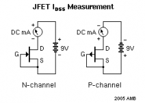
You can test them with a 9V battery:
You can test them with a 9V battery:
Attachments
Ben,
I would like to be able to test the JFets, but despite much searching, I have not found a methodology that my very limited electronic experience can work with.
If there is a guide that goes along with your diagram please point me to it. I was hoping the PEAK atlas DCA75 would suffice, but I know if doesn't give me active current through the JFets.
I have also built a new board to just do a swap out and hope for the best. As you say, not sure what else to try.
Thanks,
This will test them for operation. It will also test every other component in the amp. 
https://www.amazon.com/Mega328-Digi...mega328&qid=1628469375&sprefix=mega328&sr=8-3
As for testing for idss, the above diagram, used with a cheapie meter or an expensive one will work. Make sure you have the meter and leads configured for reading mA.
https://www.amazon.com/Mega328-Digi...mega328&qid=1628469375&sprefix=mega328&sr=8-3
As for testing for idss, the above diagram, used with a cheapie meter or an expensive one will work. Make sure you have the meter and leads configured for reading mA.
Chip,
Jim gave you a summary, I will give you an essay.
This is a good opportunity for you to expand your knowledge. Everyone starts at zero, and then learn and acquire knowledge, a bit at a time.
Schematics are not difficult. Instead of pictoral representations of components, symbols are used. So it is matter of learning what the symbols represent. And the lines joining the components are wires or pcb traces in real life.
The schematics show the test circuits for N-channel and P-channel JFETS. The 2SK170/LSK170 is N-channel and the 2SJ74/LSJ74 is P-channel. If unsure, you can look up their data sheets for that information. The data sheets also give the pin out information. Attached are the data sheets for 2SK170 and 2SJ74, so you can check the information yourself.
The pin outs are shown as drain - gate - source in that order when looking at the JFET with the flat side facing you.
So onto the schematic. The schematic in this case identifies the the drain, gate, and source on the JFET symbol. It also shows the 9V power battery with polarity, a DC meter, and finally lines that represent the wires/pcb traces that connect the components together.
So for measurement of the N-channel JFET (2SK170/LSK170), the schematic shows the negative terminal of the battery is connected to the source pin of the JFET. It also shows the gate pin is also connected to the source pin. To measure current, your meter needs to be set to ammeter mode. That usually means plugging the positive probe into Amps only jack in your meter. The schematic shows the meter negative probe is connected to the drain pin of the JFET. To complete the circuit, touch the positive probe to the positive terminal of the battery. A working JFET will show a current reading on your meter. That reading is the drain current, Idss, when Vgs (voltage between gate and source)=0. And if the JFET is functioning properly it should be the same number as what was specified by the seller, e.g. 5mA.
For P-channel JFET (2SJ74/LSJ74), follow the schematic. The difference is that the polarity of the battery and ammeter is reversed.
To connect to the JFET, you can use clip leads, some sort of small socket, or a solderless breadboard.
Also note the difference in the schematic symbol for N-channel and P-channel. You may not remember it but that is how to differentiate N-channel from P-channel if the schematic is generic with no components specified.
So that is how to do it.
And if you build a new board, after you have set the bias and output offset, use your headphone preamp first to test it. You have had the board testing properly with no preamp and then things went awry when your preamp was connected - multiple times. So try something different.
Attachments
Chip,
Jim gave you a summary, I will give you an essay.
This is a good opportunity for you to expand your knowledge. Everyone starts at zero, and then learn and acquire knowledge, a bit at a time.
Schematics are not difficult. Instead of pictoral representations of components, symbols are used. So it is matter of learning what the symbols represent. And the lines joining the components are wires or pcb traces in real life.
The schematics show the test circuits for N-channel and P-channel JFETS. The 2SK170/LSK170 is N-channel and the 2SJ74/LSJ74 is P-channel. If unsure, you can look up their data sheets for that information. The data sheets also give the pin out information. Attached are the data sheets for 2SK170 and 2SJ74, so you can check the information yourself.
The pin outs are shown as drain - gate - source in that order when looking at the JFET with the flat side facing you.
So onto the schematic. The schematic in this case identifies the the drain, gate, and source on the JFET symbol. It also shows the 9V power battery with polarity, a DC meter, and finally lines that represent the wires/pcb traces that connect the components together.
So for measurement of the N-channel JFET (2SK170/LSK170), the schematic shows the negative terminal of the battery is connected to the source pin of the JFET. It also shows the gate pin is also connected to the source pin. To measure current, your meter needs to be set to ammeter mode. That usually means plugging the positive probe into Amps only jack in your meter. The schematic shows the meter negative probe is connected to the drain pin of the JFET. To complete the circuit, touch the positive probe to the positive terminal of the battery. A working JFET will show a current reading on your meter. That reading is the drain current, Idss, when Vgs (voltage between gate and source)=0. And if the JFET is functioning properly it should be the same number as what was specified by the seller, e.g. 5mA.
For P-channel JFET (2SJ74/LSJ74), follow the schematic. The difference is that the polarity of the battery and ammeter is reversed.
To connect to the JFET, you can use clip leads, some sort of small socket, or a solderless breadboard.
Also note the difference in the schematic symbol for N-channel and P-channel. You may not remember it but that is how to differentiate N-channel from P-channel if the schematic is generic with no components specified.
So that is how to do it.
And if you build a new board, after you have set the bias and output offset, use your headphone preamp first to test it. You have had the board testing properly with no preamp and then things went awry when your preamp was connected - multiple times. So try something different.
Ben, thanks for taking the time to lay the above out. I understand it all much better. And will use it.
Also, I am going forward with a new board, just have to add the MosFets. And I will use the headphone amp to bring it online. Will report out in a few days.
- Home
- Amplifiers
- Pass Labs
- A guide to building the Pass F4 amplifier