Are you referring to Distributed Zobel Network? If yes, it is already there in my circuit.For output MOSFET oscillation mitigation, you might also look into R+C network at the MOSFET gates
"Are you referring to Distributed Zobel Network? If yes, it is already there in my circuit."
No, not an output Zobel for managing impedances on the speaker lines.
Specifically at the MOSFET gates.
See circled components in the attached screen capture from Bob's paper I mentioned.

No, not an output Zobel for managing impedances on the speaker lines.
Specifically at the MOSFET gates.
See circled components in the attached screen capture from Bob's paper I mentioned.

Yes, such Zobel chains will not interfere, the reason for their appearance is the Miller C301C401 external correction capacitors (see your diagram) and the Q303Q403 voltage amplifier transistors, which operate in hot mode. at high frequencies, the alternating voltage resistance C301C401 can become lower than the input resistance Q303Q403, which will lead to the appearance of positive feedback and an increase in output resistance, at the output of the Q501Q601 driver. An increase in the output resistance at high frequencies on the gates of Q502Q602 can unblock the parasitic capacitance between the drain and source through the gate of the Q502Q602, the Zobel R504C504 and R604C504 chain will prevent this unlocking.Exactly! This is also call a Zobel Network at the gate... As said above, my circuit already have them...
Hi Minek and othersI would use 1 pair of double-die mosfets ECW20N20 / ECW20P20.
This way they come pre-matched from the factory, no need to match them by the builder.
If using 2 pairs (single die) they will need to be matched for Vgs. Otherwise amp WILL oscillate.
i am a noob but I am a reader of this thread.
My Question:
Which color should be chosen? It is possible to get a S - Selected pair by the manufacturer. But which one should be right? In which case?
kr
Chris
Attachments
I wrote:
If you use 1 pair of double-die mosfets, you don't need to match anything, and you don't need to pay any attention to any colors.
Upper/lower devices don't need (and can't) to be matched. Only parallel devices of the same polarity need to be matched.
I would use 1 pair of double-die mosfets ECW20N20 / ECW20P20.
If you use 1 pair of double-die mosfets, you don't need to match anything, and you don't need to pay any attention to any colors.
Upper/lower devices don't need (and can't) to be matched. Only parallel devices of the same polarity need to be matched.
Good news!
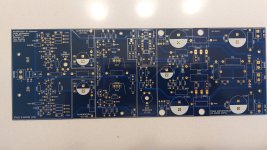
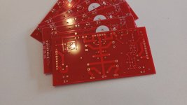
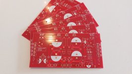
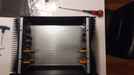
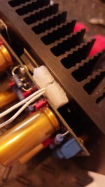
I received my PCBs. The first mechanical verification is perfect, no issue yet... I will have to make a couple of news holes in the heat-sink to screw the MOSFET and Driver transistors.
The inductor L1 is just a fast test for the required turn to get 3uH. I will redo it more nicely.
I am excited to built it!
Attachments
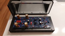
Successful progress!
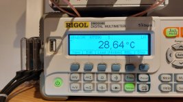
All diodes, resistors, capacitors and terminals are soldered. I tested the DC voltages of the board successfully from +/-5 VDC until +/-40 VDC by +/-5 VDC steps. I noticed a warm temperature on my fingers onto both 15 VDC Zener diode resistors R701/R801. These are 2 Watts. I measured 50 Celsius with my probe. I lowered the voltage to 35 VDC and measured only 28,64 Celsius then. I may have to raise the power of these resistors.
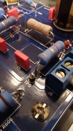
I noticed a bad design placing of my TP5 that is very close to the resistor R13 pin connected to the capacitor C4. I guess I tried to be to much symmetric and didn't noticed this proximity. There is a risk to short the resistor pin with the oscilloscope ground alligator. Nothing dangerous until you connect the alligator there!
I will start the IPS transistors installation tomorrow and make other tests...
All diodes, resistors, capacitors and terminals are soldered. I tested the DC voltages of the board successfully from +/-5 VDC until +/-40 VDC by +/-5 VDC steps. I noticed a warm temperature on my fingers onto both 15 VDC Zener diode resistors R701/R801. These are 2 Watts. I measured 50 Celsius with my probe. I lowered the voltage to 35 VDC and measured only 28,64 Celsius then. I may have to raise the power of these resistors.
I noticed a bad design placing of my TP5 that is very close to the resistor R13 pin connected to the capacitor C4. I guess I tried to be to much symmetric and didn't noticed this proximity. There is a risk to short the resistor pin with the oscilloscope ground alligator. Nothing dangerous until you connect the alligator there!
I will start the IPS transistors installation tomorrow and make other tests...
Attachments
* * * G O O D N E W S * * *
This new PCB is a total success!
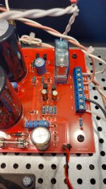
I easily fix the TP5 mechanical problem like this:

At first, after the IPS was build, I found no problem. Then I built-ed the VAS and got a distorted square wave showing at the IPS output. I decided then to build the BIAS Spreader thinking that it would be necessarily but same problem.
So I build the OPS without the MOSFETs. The output was nice at the OPS but I still had two square waves at the IPS outputs. So I slept on it. This morning, seeing that I did all my tests at +/-35 VDC instead of the original design +/-55 VDC, I decided to try to lower the voltage to +/-35 VDC in LTSpice. No square wave on simulation. Then I thought... I don't have MOSFET in real. I deleted the MOSFET in LTSpice and surprise! I got a square wave at the IPS output!
So I choose to solder the two OPS MOSFETs and Bing! A superb sinusoidal at both IPS outputs.
I started all the usual tests with success. I raised the input voltage to 1.6Vpp without apparent distortion. Then I checked the frequencies from 1 Hz to 100 kHz at 356mV:
10 Hz:

1 kHz:

10 kHz:

20 kHz:

I did a couple of Bode plot without charge and with an 8 Ohms resistor.
Without any charge 10 Hz, phase =-13.27 deg.

Without any charge 1 kHz, phase =-0.49 deg.

Without any charge 30 kHz, phase =-1.88 deg.

Then with 8 Ohms/50 Watts resistor. Forget the phase of 166.37 deg at 10 Hz, This is a bug in my scope that happen sometime when it start. A second plot would get other result. I usually restart the plot when I really want to get ride of the bug aesthetically...

This one is the FFT curve with the 15 first peaks of distortion:

Tomorrow I will make distortion tests in my REW software on the PC...


This new PCB is a total success!
No serious mechanical problem found
No electrical problem found
No oscillation
0 VDC at the output
No parts that heat over their range
A third harmonic 62.39dB below the 1kHz fundamental
A second harmonic 63,88dB below the 1kHz fundamental
I am a happy guy!I easily fix the TP5 mechanical problem like this:
At first, after the IPS was build, I found no problem. Then I built-ed the VAS and got a distorted square wave showing at the IPS output. I decided then to build the BIAS Spreader thinking that it would be necessarily but same problem.
So I build the OPS without the MOSFETs. The output was nice at the OPS but I still had two square waves at the IPS outputs. So I slept on it. This morning, seeing that I did all my tests at +/-35 VDC instead of the original design +/-55 VDC, I decided to try to lower the voltage to +/-35 VDC in LTSpice. No square wave on simulation. Then I thought... I don't have MOSFET in real. I deleted the MOSFET in LTSpice and surprise! I got a square wave at the IPS output!
So I choose to solder the two OPS MOSFETs and Bing! A superb sinusoidal at both IPS outputs.
I started all the usual tests with success. I raised the input voltage to 1.6Vpp without apparent distortion. Then I checked the frequencies from 1 Hz to 100 kHz at 356mV:
10 Hz:
1 kHz:
10 kHz:
20 kHz:
I did a couple of Bode plot without charge and with an 8 Ohms resistor.
Without any charge 10 Hz, phase =-13.27 deg.
Without any charge 1 kHz, phase =-0.49 deg.
Without any charge 30 kHz, phase =-1.88 deg.
Then with 8 Ohms/50 Watts resistor. Forget the phase of 166.37 deg at 10 Hz, This is a bug in my scope that happen sometime when it start. A second plot would get other result. I usually restart the plot when I really want to get ride of the bug aesthetically...
This one is the FFT curve with the 15 first peaks of distortion:
Tomorrow I will make distortion tests in my REW software on the PC...
Attachments
I did Slew Rate tests this morning, and I also did THD tests with my REW software. For the latest, I have to take them with reserve because the maximum line voltage of my Focusrite Scarlett 2i2 external audio card is +22dBu at the minimal gain level. In order to use it to test the amp THD with the REW software, I had to limit the input voltage to 50 mV. That is for sure not the maximum output voltage of the amp! Still, the THD is always below the noise level of the Scarlett 2i2, and also this card is limited to 20 kHz.
Here are the Slew Rate at 1 kHz and 20 kHz. The yellow trace is the input from my generator, the magenta and light cyan trace are the IPS1 and IPS2 outputs, cyan is hidden behind magenta, and blue trace is the output:


And here are the four THD screenshots, with 2nd order, 3rd order, Total THD and Noise Floor highlighted. All the grey traces are below the noise floor:
2nd order highlighted:

3rd orderr highlighted:

THD highlighted:

Noise Floor highlighted:

And two last screenshots showing the bandwidth from 1 Hz to 20 kHz, with the phase:
Bandwidth highlighted:

Phase highlighted:

Here are the Slew Rate at 1 kHz and 20 kHz. The yellow trace is the input from my generator, the magenta and light cyan trace are the IPS1 and IPS2 outputs, cyan is hidden behind magenta, and blue trace is the output:
And here are the four THD screenshots, with 2nd order, 3rd order, Total THD and Noise Floor highlighted. All the grey traces are below the noise floor:
2nd order highlighted:
3rd orderr highlighted:
THD highlighted:
Noise Floor highlighted:
And two last screenshots showing the bandwidth from 1 Hz to 20 kHz, with the phase:
Bandwidth highlighted:
Phase highlighted:
Hi,
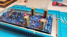
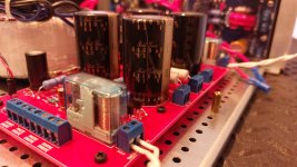
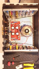
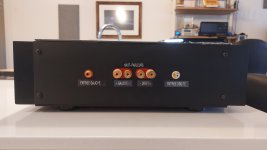
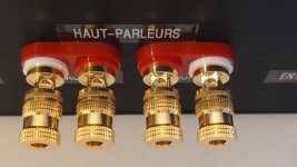
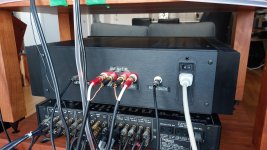
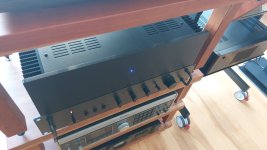
I have finished my DIY amplifier. I made a PCB for the Power Supply and the speakers protection circuit. The latest based from the schematic of figure 8.15 of G. Randy Slone book "High-Power Audio Amplifier Construction Manual".
The amplifier is working like a charm and I am very proud of my PCB designs, both the audio one and the Power Supply/Protection one.
I want to thank every one who took the time to help and answer all my questions.
This is great!
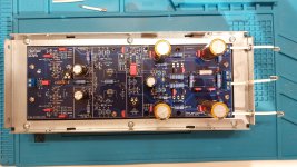
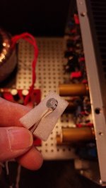
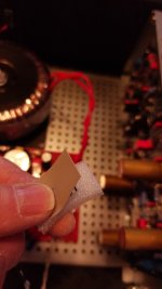
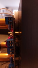
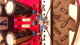
Some pictures...
I have finished my DIY amplifier. I made a PCB for the Power Supply and the speakers protection circuit. The latest based from the schematic of figure 8.15 of G. Randy Slone book "High-Power Audio Amplifier Construction Manual".
The amplifier is working like a charm and I am very proud of my PCB designs, both the audio one and the Power Supply/Protection one.
I want to thank every one who took the time to help and answer all my questions.
This is great!
Some pictures...
Attachments
-
 20240328_125722.jpg272.9 KB · Views: 40
 -
 20240328_125714.jpg348 KB · Views: 43
 -
 20240327_123317.jpg307.2 KB · Views: 39
 -
 20240302_201902.jpg280.9 KB · Views: 45
 -
 20240302_201533.jpg308.8 KB · Views: 42
 -
 20240330_101714.jpg422.6 KB · Views: 40
 -
 20240330_101718.jpg400.9 KB · Views: 35
 -
 20240402_113225.jpg356.4 KB · Views: 35
 -
 20240402_115123.jpg226.1 KB · Views: 35
 -
 20240402_115207.jpg205.3 KB · Views: 35
 -
 20240402_120014.jpg276.2 KB · Views: 31
 -
 20240402_120036.jpg193 KB · Views: 36
 -
 20240402_152653.jpg457.8 KB · Views: 43
 -
 20240402_161009.jpg536.1 KB · Views: 45
 -
 20240402_161042.jpg355.5 KB · Views: 43
 -
 20240309_130153.jpg155.3 KB · Views: 33
 -
 20240309_130300.jpg263.2 KB · Views: 36
 -
 20240329_125308.jpg453.1 KB · Views: 32
 -
 20240329_125316.jpg240.3 KB · Views: 45
Thank you minek123 and chermann!Which post has the final schematic ('as built') ?
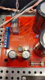
Here are the two final drawings in PDF format. The Amplifier and the Power Supply+Protection Circuit. In the Amplifier schematic, I replaced the two resistors R701 and R801 from 3 W MF for 5 W MF.
Yesterday I wanted to test the 20 kHz square wave but the DC Detection section in the Protection circuit start to engage around 9~10 kHz. The relays was triggered (openning contacts), than returning to close, and triggered again, in a constant frequency. I guess this is normal as the wave coud be perceaved as a high or low DC level at this hight frequency.
Also, the LED diode of the protection circuit is supposed to have 4 states from the book explanation. The LED is supposed to blink slowly for around two seconds on Power On. Then it stop to blink and stay on while the speakers relays engage. This is working fine. But if one of the two Thermal Switch open, when one of the heatsink reach +90 °C, or if a DC presence of 1.7 VDC is present on the speakers, the LED should blink rapidly and the relays should open. Although both function work as expected, the LED in this state is flashing so fast that it seem almost on and it's is not really distingeable as a fault state. Before making the PCB I tested the circuit on a proto-board and I never find the right condensators/resistors combination to slow down this state.
Attachments
- Home
- Amplifiers
- Solid State
- A Lateral MOSFET Power Amplifier Design (second try)