Hi there,
This instrument is designed to measure the thermal resistivity of interface materials like Sil-pads or micas, and thermally conductive compounds like silicone or metal pastes.
It supersedes a very crude jig I already built, which was rudimentary, inaccurate, required manual balancing and computations and had a poor repeatability.
It was (barely) sufficient for an occasional use, but since I wanted to carry out more systematic tests on a number of materials, I needed something more convenient and deterministic.
So, I embarked on designing this one: it doesn't have the ambition of absolute accuracy measurements (thermal measurements aren't especially simple), but it is automatic, fast, convenient and easy to use.
The main goals are:
a)Being able to rank accurately various materials ie. material A is better than B, which itself is better than C.
b)Being able to quantify the difference between materials: ie. material A has a thermal resistivity 10% lower than B.
The value displayed is indicative, "best effort": I tried to make an as good job as possible, but I lack adequate calibration means and exact knowledge of the thermal behavior of the components I used, so I sometimes used educated guesses instead.
The principle of operation is quite straightforward: a heater generates a constant and calibrated flux of power through the interface to be measured, and the temperature of each side is measured and translated into thermal resistivity.

Of course, the practical implementation is somewhat more complicated, because I cannot afford the luxury of custom parts like separate heater and sensors, and because thermal objects are largely imperfect: unlike their electrical counterparts, thermal conductors and insulators are not extremely different: both are "semiconductors" of varying degrees.
The mechanical and thermal aspects are therefore essential, in particular to achieve a good repeatability.


To be continued...
This instrument is designed to measure the thermal resistivity of interface materials like Sil-pads or micas, and thermally conductive compounds like silicone or metal pastes.
It supersedes a very crude jig I already built, which was rudimentary, inaccurate, required manual balancing and computations and had a poor repeatability.
It was (barely) sufficient for an occasional use, but since I wanted to carry out more systematic tests on a number of materials, I needed something more convenient and deterministic.
So, I embarked on designing this one: it doesn't have the ambition of absolute accuracy measurements (thermal measurements aren't especially simple), but it is automatic, fast, convenient and easy to use.
The main goals are:
a)Being able to rank accurately various materials ie. material A is better than B, which itself is better than C.
b)Being able to quantify the difference between materials: ie. material A has a thermal resistivity 10% lower than B.
The value displayed is indicative, "best effort": I tried to make an as good job as possible, but I lack adequate calibration means and exact knowledge of the thermal behavior of the components I used, so I sometimes used educated guesses instead.
The principle of operation is quite straightforward: a heater generates a constant and calibrated flux of power through the interface to be measured, and the temperature of each side is measured and translated into thermal resistivity.
Of course, the practical implementation is somewhat more complicated, because I cannot afford the luxury of custom parts like separate heater and sensors, and because thermal objects are largely imperfect: unlike their electrical counterparts, thermal conductors and insulators are not extremely different: both are "semiconductors" of varying degrees.
The mechanical and thermal aspects are therefore essential, in particular to achieve a good repeatability.
To be continued...
Attachments


Last edited:
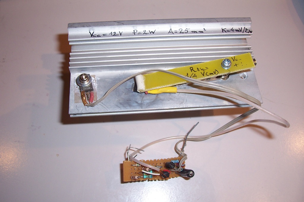
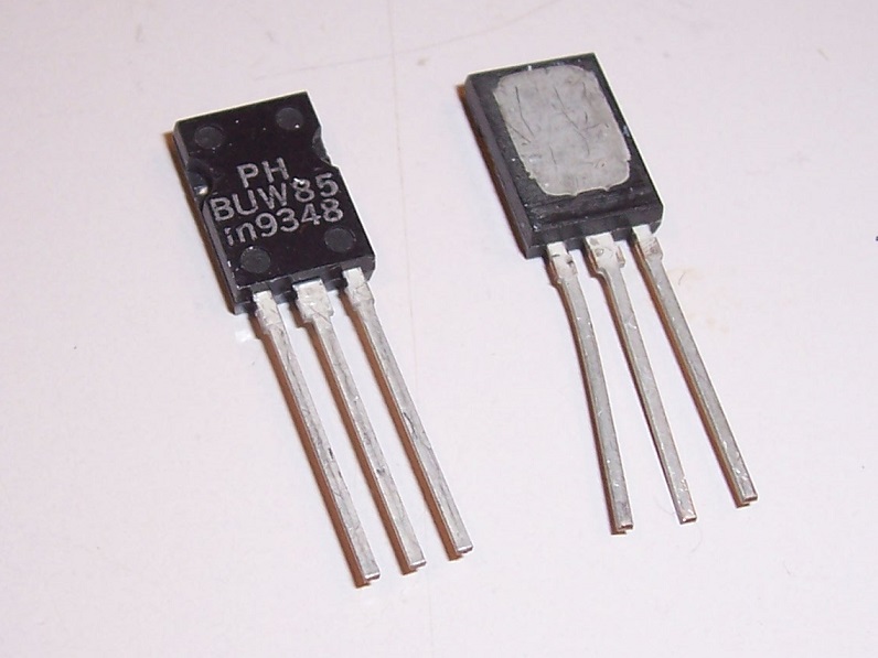
The single most important component choice of this design is certainly the heater/sensor transistor.
Its thermal, mechanical and electrical characteristics will influence heavily the level of performance attainable
I opted for a BJT, because it easily allows for simultaneous power generation and temperature measurement, via the Vbe.
Ideally, the case has to be reasonably small (to be able to test smallish samples), must not have complicated shapes (to make the clamping simple and reliable), has to have one side completely devoted to the metal mounting base, and its thermal resistance Rtj-mb must be small.
The SOT82 case fulfills most of these requirements:

In addition, there are also electrical and thermal consideration: the power generated is relatively high: 6.67W.
This means a high U*I product, but using a high current would be problematic: it requires a thick enough emitter wire (not because of the losses themselves, but because of the errors it causes to the measured Vbe voltage), but such a thick wire would cause additional, uncontrolled thermal leaks directly to the ambience.
The solution is to use a relatively high voltage, ~100V for example.
Of course, the transistor must have sufficient Vceo and SOA for that; this mandates a HV transistor.
A transistor that fits the bill is the BUW85:
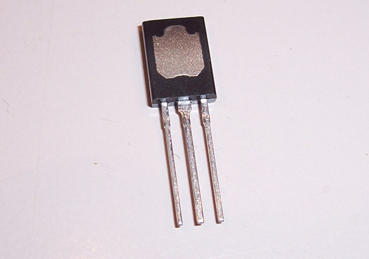
Note that not all SOT82 transistors are suitable: the mounting base of a 2SB1168 is unsuitable:
The BUW85 is a good starting point, but it requires improvements: the flatness of the mounting base is certainly sufficient for normal application, but for metrology, you'd want something better.
There is also a bit of creep of the molding compound on the metal.
For these reasons, I lapped the surface.
I also removed ~0.1mm of the epoxy surrounding the metal: the epoxy is a poor heat conductor compared to metal, but it is comparable to many interface materials, and it would thus change the apparent surface depending on the material tested: poor materials would look better than they really are.
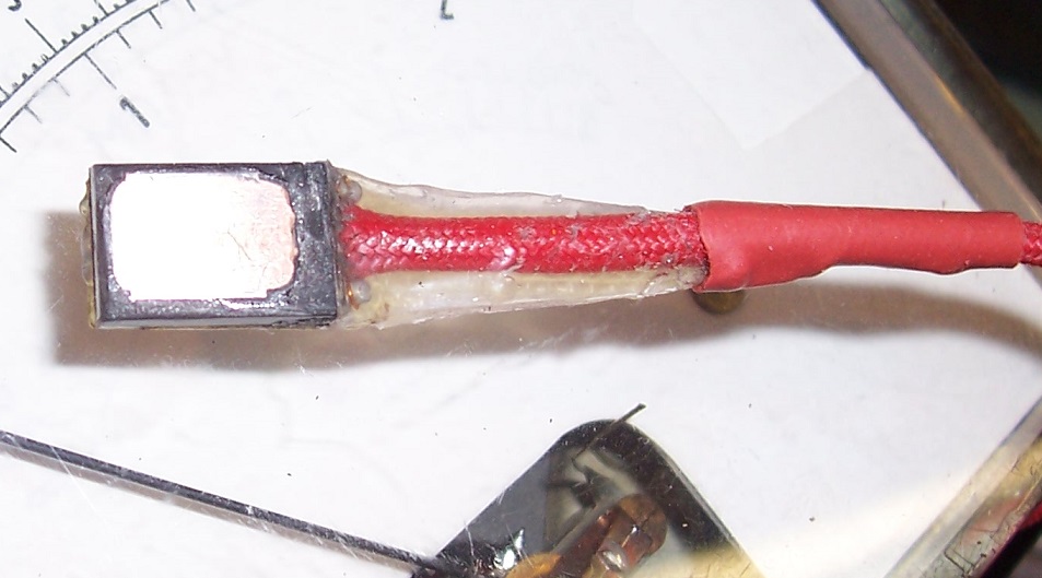
Finally, I covered the top side with a blade of thin epoxy composite, to act as a strain relief for the wires, and also as a reinforcement, to spread the tensions applied to the epoxy case:
Here is the power supply:
http://www.diyaudio.com/forums/attachment.php?attachmentid=678022&d=1525170097
Its thermal, mechanical and electrical characteristics will influence heavily the level of performance attainable
I opted for a BJT, because it easily allows for simultaneous power generation and temperature measurement, via the Vbe.
Ideally, the case has to be reasonably small (to be able to test smallish samples), must not have complicated shapes (to make the clamping simple and reliable), has to have one side completely devoted to the metal mounting base, and its thermal resistance Rtj-mb must be small.
The SOT82 case fulfills most of these requirements:
In addition, there are also electrical and thermal consideration: the power generated is relatively high: 6.67W.
This means a high U*I product, but using a high current would be problematic: it requires a thick enough emitter wire (not because of the losses themselves, but because of the errors it causes to the measured Vbe voltage), but such a thick wire would cause additional, uncontrolled thermal leaks directly to the ambience.
The solution is to use a relatively high voltage, ~100V for example.
Of course, the transistor must have sufficient Vceo and SOA for that; this mandates a HV transistor.
A transistor that fits the bill is the BUW85:
Note that not all SOT82 transistors are suitable: the mounting base of a 2SB1168 is unsuitable:
The BUW85 is a good starting point, but it requires improvements: the flatness of the mounting base is certainly sufficient for normal application, but for metrology, you'd want something better.
There is also a bit of creep of the molding compound on the metal.
For these reasons, I lapped the surface.
I also removed ~0.1mm of the epoxy surrounding the metal: the epoxy is a poor heat conductor compared to metal, but it is comparable to many interface materials, and it would thus change the apparent surface depending on the material tested: poor materials would look better than they really are.
Finally, I covered the top side with a blade of thin epoxy composite, to act as a strain relief for the wires, and also as a reinforcement, to spread the tensions applied to the epoxy case:
Here is the power supply:
http://www.diyaudio.com/forums/attachment.php?attachmentid=678022&d=1525170097
Attachments


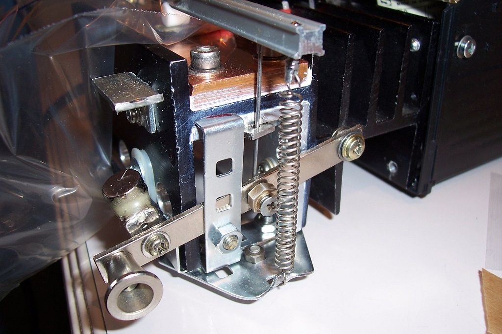
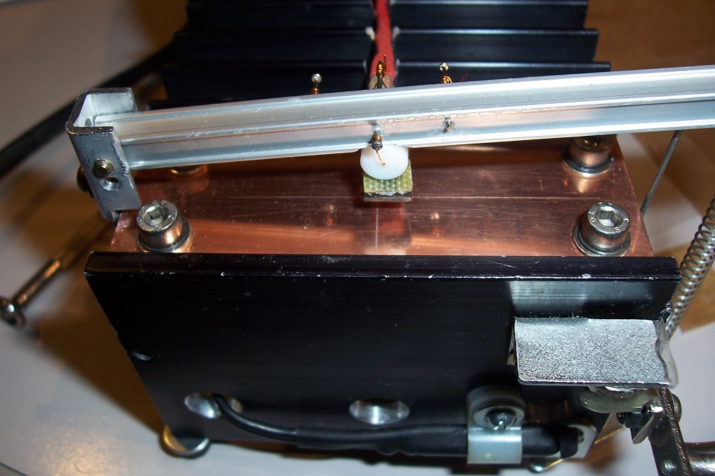
Thermal aspects:
The test surface is a 6.5mm thick slab of polished copper.
The reasons for something that massive are twofold: to provide a completely isothermal reference plane of negligible thermal resistivity compared to any object tested, and to provide a large thermal "flywheel", thanks to its thermal capacity.
This capacity is supplemented by the main heatsink, and is further fortified by an additional L-shaped aluminum profile. The profile also reduces the thermal impedance to the rest of the heatsink.
Paradoxically, the large thermal mass and its commensurately high time constant are essential to the speed of the instrument: even with the relatively high 6.67W input power, the rate of temperature rise is very slow, something like 1°C/min.
Small rates cause correspondingly small temperature gradients, meaning the reference sensor will always stay almost synchronous with the heater sensor.
This would not necessarily be the case, even if the thermal resistance between the heater and sensor is low: the thermal capacity of the transmitting medium means time-lag/transmission line effects, and with high dT°/dt, this would cause errors.
The reference sensor is not only in direct contact with the rear side of the copper, but it is also completely embedded in the heatsink, in a cavity milled in its thickness; even the screw is enclosed into the L-profile.
Since the power flux to and from this transistor are negligible, it is completely isothermal with the H.S.
In fact, in this setup, the settling time is essentially dictated by the time constant of the heater wrt. the reference surface:
when the power is first applied, the die heats up very quickly (in around 1ms or so), then it begins to heat the mounting base, and finally the more remote parts of the heater transistor, epoxy, etc.
The longest time constant is therefore the product of Rt(j-heatsink) and the heat capacity of the SOT82 package.
When the transistor is directly in contact with the heatsink, the residual thermal resistance is 2°C/W, and the settling time is very fast, a few seconds, and when the thermal interface is at the maximum possible, 16°C/W (equivalent to 8°C.cm²/W), the settling time rises to 10~15s, which remains perfectly acceptable for thermal measurements.
The top side of the slab receives the sample and the heater transistor, whilst the sensor is screwed directly underneath. The position is materialized by cross-hairs engraved on the copper surface.
The copper surface has been polished without particular precaution: as the test surface is much smaller than the slab, global flatness or convexity/concavity issues are of no concern.
Matters are different for the heater: it is much smaller, and properly hand-lapping such a small object is notoriously difficult.
As I didn't want to invest in specialized lapping material for just a one-off, I developed a very specific method requiring practically no equipment. I can describe it, if someone is interested (but it is only applicable in this very case though).
The heater is pressed onto the heatsink by a spring and lever system: in its nominal position, the spring exerts a force of 10.5N on the lever, resulting in a force of 25N at the transistor level; as the active area is 0.5cm², this causes a pressure of 50N/cm², or 500kPa, a neat and round number.
It is also OK for reproducible and meaningful tests, without endangering the integrity of the heater transistor.
The clamping force is applied through a self-centering PTFE roller, in order to ensure a smooth and uniform pressure.
Note that for good surface condition and sufficient pressure, the pressure influence becomes minimal: manually interfering with the pressure has practically no influence, except for samples having a structured and deformable surface, like some Silpads having a woven fiber-glass skeleton.
When the lifting mechanism is released, it becomes completely disconnected mechanically, and doesn't interfere with this value.
The lifting lever also automatically disables the heater, for safety and productivity reasons (an independent overtemperature protection circuit is also included)
The heater transistor choice obeys a well-defined rationale, see above posts, but what about the two other transistors, BF458 and BSS38?
After having selected the BUW85, I had to find two other transistors that matched its thermal characteristics as closely as possible.
I tried using spice sims, but it was a complete disaster, and I ended up using the good old trial and error method.
These two transistors emerged as winners after many rounds of competition...
Almost any other type would be usable, but they would need additional scale and offset adjustments, not a very pleasant perspective.
This pic shows the setup during the calibration of the zero Rth situation:
Attachments

Last edited:
Thanks!Bravo!
Corrections and compensations:
In a thermal test setup, there are numerous sources of errors. In this instrument, only two of them, the most blatant ones are explicitly addressed.
Some others are implicitly catered for by the stasis built into the design: the voltage, current and thus the power to the heater are tightly controlled; this means that a number of errors end up looking like offset errors, which can be eliminated during the normal calibration procedure.
The most severe error is caused by the thermal resistance of the heater transistor itself, the Rtj-mb, stated as 2°C/W in the datasheet.
Fortunately, it is also the easiest to compensate: one just has to adjust the final display offset to read zero in a zero Rth situation, in practice with the heater directly in contact with the reference surface, helped by silver thermal paste.
There are theoretical objections to this method: a thermal contact resistance is never zero, and the small residual amount will be eliminated by the procedure, meaning the reading will always be slightly better than the actual, absolute thermal resistivity.
Is it a problem? I don't think so, as long as you are aware of the way the measurement is done. You can also reformulate the definition of the value displayed: it is the difference between the best practical Rth possible without the sample and that with the sample; it will be very small anyway.
On the schematic, the offset correction is carried out by R22, but it seems to have an inverted polarity, ie. it acts as though the Rtj-mb is negative, which is nonsense of course: initially the (positive) correction voltage was added in series with R21, but when the prototype was built, I realized that the parameters discrepancies between the heater and the reference already overcompensated the 2°C/W, but as there was no negative supply provisioned, I had to find a not too awkward way of adding the offset without disrupting too much the balance of the circuits, which is why it is derived from the 100V supply with the 10 Meg resistors. I had been fooled by the spice sims...
The other correction takes into account the fact that the heater transistor will lose some heat to the ambience, even though it is attached to a heatsink: due to its thermal resistance and that of the sample, it will be significantly hotter than the ambience, at the very least 2°C/W*6.67W=13.3°C.
The heat leaked there will be subtracted from that flowing through the interface, leading to some (relatively minor) errors.
According to the datasheet, the naked transistor has a thermal resistance of 100°C/W, but here one full side of the case is devoted to the heatsink, and will not participate to the losses; however, some of the losses will be directly to the heatsink, bypassing the interface under test.
All of this is reflected in the coefficients I attributed following educated guesses: R46 implements a power increase corresponding to 150°C/W of global losses, and the divider R40/R41 implements a 2:1 ponderation factor between the losses to the ambience and the bypassing of the sample.
All of this is wild speculation of course, but it cannot be too far off the reality, and doing something in the right direction is always going to be better than doing nothing. The absolute numerical impact will remain small anyway.
Here are some pics of the circuit:
Attachments


That is quite some effort!!! Well done.
Have you had time to check repeatability of measurements to give some insight in to that tolerance?
I guess the use of a PTFE cylinder to apply pressure along a mid-line to the top of the package is akin to many spring steel device mounting clips that similarly apply pressure along a 'line'.
For the zero Rth situation, with no interface material, would a regression line of results using steps of heater power be enlightening? I guess a custom 'cover' made of thermal insulation over the heater transistor may show up some measurement value change due to local convection, but wouldn't influence transistor lead conduction loss.
Can you elaborate on why you needed a measurement jig for starters? Were you interested in performance of interfaces that had no datasheet levels, or wanted to assure yourself of datasheet levels, or ...?
Yes: for dry surfaces, multiple identical measurement result in a dispersion of a few percents either side, proportionately larger for low Rt values.Have you had time to check repeatability of measurements to give some insight in to that tolerance?
For greased or soft surfaces (silicone f.e.), variations become mostly unnoticeable
Yes, that is exactly the ideaI guess the use of a PTFE cylinder to apply pressure along a mid-line to the top of the package is akin to many spring steel device mounting clips that similarly apply pressure along a 'line'.
The problem with changing the power is that it requires a full realignment each time, offset, gain, correction, making the idea rather difficult to apply.For the zero Rth situation, with no interface material, would a regression line of results using steps of heater power be enlightening? I guess a custom 'cover' made of thermal insulation over the heater transistor may show up some measurement value change due to local convection, but wouldn't influence transistor lead conduction loss.
In fact, the instrument only has one true range: the pseudo-ranges are fabricated by changing the magnification ratio of the display.
True ranges would mean switching the power level too, but then things become much more complicated, because each power step needs to have its individual adjustments
In fact, had I had the possibility of changing the power easily, I would certainly have done it already: when the instrument was finished, it worked rather better than I had imagined for the low Rth/high resolution cases, meaning a test power of 2~2.5W would have been sufficient, allowing a range of 25°C.cm²/W, useful for testing thicker insulating materials, like PCB's.
With 8°C.cm²/W, I can only test up to moderately poor materials (limited by the die temperature)
I was certainly not trying to make quality controls on commercial products (Which BTW are in good agreement with values displayed): my goals are to test "improvised materials": "parchment" baking paper, oven bags films, siliconized sticker backing paper, to name a few, and to brew some of my own.Can you elaborate on why you needed a measurement jig for starters? Were you interested in performance of interfaces that had no datasheet levels, or wanted to assure yourself of datasheet levels, or ...?
Note that some of the examples I gave are on a par or outperform most standard-quality dedicated products.
I wouldn't trust them for 1kV or difficult environments, but for low-voltage transistor circuits, they should be perfectly OK.
Here is the thermal equivalent circuit of the tester:
Attachments

Seriously good jig, and interesting to appreciate the nuances 🙂
How does the base heat spreader change with temperature at the spreader, given that at best it is an infinite heatsink? The comment above suggests that was 1 degC per minute.
When you did the multiple identical measurements, were they done by opening the jig and reseating the DUT interface each time, or just waiting some time between measurements for the jig to cool, or was that repeated with no cooling time (which begs the query about how long can a test be run before some measurement deviation occurs)?
1°C/min is approximate, and is the starting rate of the exponential.How does the base heat spreader change with temperature at the spreader, given that at best it is an infinite heatsink? The comment above suggests that was 1 degC per minute.
The ~final temperature of +17°C relative to the ambience is reached after some tens of minutes, and the thermal resistance of the whole heatsink assembly, as seen from the spreader is a little under 2.5°C/W
I made these tests in a relatively quick succession, the time to open the jig and reposition the sample, which means they are relevant to mechanical uncertainties rather than thermal ones.When you did the multiple identical measurements, were they done by opening the jig and reseating the DUT interface each time, or just waiting some time between measurements for the jig to cool, or was that repeated with no cooling time (which begs the query about how long can a test be run before some measurement deviation occurs)?
I now just made a purely thermal stability test: I placed a sample giving a near-full scale reading with the jig in a completely cold condition (~24°C here), and observed the evolution until the settling was complete (without changing anything else): there were minute deviations, first in the positive direction, then negative, and eventually, when the settling was complete, the reading returned to its initial value, but this is probably more fortuitous luck than anything else, and is completely insignificant anyway, because the p-to-p variation during the whole process was less than 1%, significantly better than the resolution/repeatability/accuracy to be expected from this setup.
The minor oscillations could be caused by a number of factors: calibration errors or mistracking between the sensors, heating of the electronics inside the box, time-constants of loosely coupled distant parts, variation of the thermal resistance itself, etc
Anyway, thermal drift issues do not seem to present a major obstacle: mechanically-induced uncertainties are dominant here, which comes as no surprise, as the mechanical design is a bit crude (for a purist), with brass-to aluminum pivots, degrees of freedom missing, trigonometric approximations, etc.
Last edited:
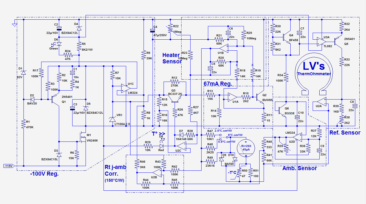
Here is a circuit description:
For two reasons: with a NMOS as a pass element, which is the most obvious option for cost, performance, robustness and silicon efficacy, a negative regulator is required if the dropout voltage is to be kept within reasonable bounds.
In fact, this regulator is actually an LDO one, and with a better MOS than the VN2406, the dropout voltage could be brought well below 100mV, but such a performance is absolutely not required here: less than 1V is quite sufficient.
The other reason is that a negative regulator has its ground natively positive, and for safety reasons, the collectors of the two sensor transistors have to be grounded, at the same potential as the heatsink.
Of course, it is always possible to play with floating supplies to accommodate any situation, but doing things in a direct and straightforward manner is simpler.
The circuit is rather classical, with U1C as an error amplifier, except for one or two details: as the regulator circuitry is referenced to the output, a voltage translator Q1 is required, and for the same reason, a start-up circuit composed of D1/D2/R1 is also needed.
Finally, the feedback divider R8/R9 also receives a correction voltage derived from the temperature values: the voltage is increased to keep the power-flux through the interface constant, even if the losses to the ambience are increased due to an elevated temperature of the heater transistor.
Two 12V auxiliary supply voltages are derived from the main 100V via shunt regulators: one is referenced to the (positive) ground and supplies the translator of the reference sensor, whilst the other is output referenced and supplies all the processing circuits and the 100V regulator itself.
The raw DC input is provided by a voltage quadrupler operating from a 24V transformer, but that was dictated purely by the availability of components: I didn't have an 80V transformer of suitable power handy, and I resorted to this expedient, but anything providing >105V @ 100mA DC would be perfectly suitable.
If the input voltage is really high, like 150V, a hefty heatsink will be required for M1, but that's just common sense...
- -100V Regulator
For two reasons: with a NMOS as a pass element, which is the most obvious option for cost, performance, robustness and silicon efficacy, a negative regulator is required if the dropout voltage is to be kept within reasonable bounds.
In fact, this regulator is actually an LDO one, and with a better MOS than the VN2406, the dropout voltage could be brought well below 100mV, but such a performance is absolutely not required here: less than 1V is quite sufficient.
The other reason is that a negative regulator has its ground natively positive, and for safety reasons, the collectors of the two sensor transistors have to be grounded, at the same potential as the heatsink.
Of course, it is always possible to play with floating supplies to accommodate any situation, but doing things in a direct and straightforward manner is simpler.
The circuit is rather classical, with U1C as an error amplifier, except for one or two details: as the regulator circuitry is referenced to the output, a voltage translator Q1 is required, and for the same reason, a start-up circuit composed of D1/D2/R1 is also needed.
Finally, the feedback divider R8/R9 also receives a correction voltage derived from the temperature values: the voltage is increased to keep the power-flux through the interface constant, even if the losses to the ambience are increased due to an elevated temperature of the heater transistor.
Two 12V auxiliary supply voltages are derived from the main 100V via shunt regulators: one is referenced to the (positive) ground and supplies the translator of the reference sensor, whilst the other is output referenced and supplies all the processing circuits and the 100V regulator itself.
The raw DC input is provided by a voltage quadrupler operating from a 24V transformer, but that was dictated purely by the availability of components: I didn't have an 80V transformer of suitable power handy, and I resorted to this expedient, but anything providing >105V @ 100mA DC would be perfectly suitable.
If the input voltage is really high, like 150V, a hefty heatsink will be required for M1, but that's just common sense...
Last edited:
- Temperature sensors
There are two main techniques for using a transistor (junction) as a temperature sensor: one is to directly rely on the negative tempco of the Vbe to derive the temperature value, like in a base-spreader for instance, and the other is based on the Vbe difference when the bias current is switched between two values.
The direct Vbe method is simple and easy to implement, but the final tempco depends on various technological parameters and an individual calibration is required for each component.
The two-current method is based on first principles and its result is largely independent from component variation; it is thus the golden standard of temperature measurement.
The choice between the two looks like a no-brainer, and guess what?
I picked the lesser option...
Why?
For a number of reasons: the two-current method is significantly more complicated for sure, and it has to be dupicated two times (triplicated?) because the tester uses three sensors.
This wouldn't have frightened me: I can manage complexity if it serves a meaningful purpose.
Another problem is to keep the average dissipation of the heater/sensor transistor constant whilst switching its base current; it is manageable.
The real issue is the third one: in the two-current method, the temperature of the sensor needs to be kept accurately constant, otherwise the variation caused by the negative tempco will swamp and corrupt the measurement.
When the power dissipated by the sensing transistor is negligible (which is normal practice), this poses no problem, but here 6.67W is dissipated in this transistor, and as soon as the heating is removed, the die very quickly reaches an equilibrium with its direct thermal surroundings, because of its tiny thermal capacity.
How quickly? It depends on the parts you consider, but it in the hundreds of µs region, and you have to be much faster than the thermal time constant if the measurements require great accuracy, which is the case here.
This means that the low-current phase cannot last longer than a few µs. This in turn makes the electrical side of things challenging, because you have to deal with the inductance of connection, the inherent slowness of HV devices, etc.
For power switching purposes, the BUW85 is reasonably fast, but for accurate metrology, you need to look at the last tenths of % of the settling time, and such a transistor has many regions in which it can store minutes amount of charge. These effects are normally totally irrelevant but in such an application, they become a headache.
Nothing insurmountable of course, but the cost/benefit equation ends up tilting in favor of the simpler solution, which is why I opted for it.
It means adjustments and calibration, but the more evolved solution would have involved trailing compensations, etc., thus no better in my opinion.
For those interested, here is a description of the two methods discussed:
https://www.onsemi.com/pub/Collateral/AND8494-D.PDF
Last edited:
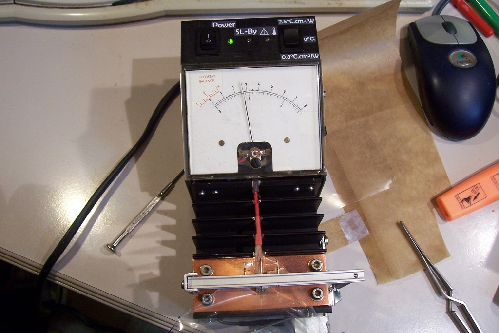
- Display, overtemp safety and calibration
I used an analogue meter to display the measurement result: it is not only inherently differential, but it also allows for an easy implementation of multiple ranges by switching a single resistor, and it is pleasant and intuitive to look at and to use.
Many other alternatives are of course possible, but since high resolution or accuracy is not needed here it is perfectly sufficient.
I went as far as compensating the tempco of the copper with a NTC, but that's icing on the cake, even for the most sensitive range.
The meter is connected to measure the difference between the heater temperature and the reference sensor, which monitors the copper reference surface.
The ambient sensor does not directly intervene in the measurement, it simply corrects the power flux generated by the heater.
All the conditioners of the sensors are calibrated to deliver 10.0mV/°C: the outputs of U1B, U2A and U2D.
Because the 6.67W dissipated could easily fry an uncooled BUW85 in a matter of seconds, some means of protection is required: U2C monitors the heater sensor's output, and when it reaches a voltage corresponding to 140°C, it greatly reduces the dissipation by switching the current value via Q3.
It also lights the temperature alarm LED.
Some hysteresis is provided by R28, and the rest by the reduced Vbe voltage resulting from a lower current.
In practice, this results in a thermal multivibrator having a period of some tenths of Hz when the BUW is insufficiently cooled.
Here is an outline of the calibration philosophy:
All three sensors are thermally bound to the copper slab: the reference sensor is already in the correct situation, the BUW is placed directly in contact with the help of silver paste and the ambient sensor is taped to the heatsink and thermally insulated, which is imperfect but sufficient considering its minor role.
The first thing to do is to calibrate the heater for exactly 10.0mV/°C.
The copper temperature is measured thanks to a thermocouple directly inserted into the slab through a 1.5mm service-hole.
Because the heater itself is incapable of raising the temperature very much or very quickly, an additional 25W resistor is bolted to the heatsink, to improve the speed and resolution: the "low" temperature is the ambience, between 20 and 25°C, helped by a fan, and the "high" temperature is 60°C.
From there and the voltage readings at the output of U1B, it is easy to deduce the tempco, and compute the suitable resistors value of R18 and R19 (to be confirmed by another temperature sweep, of course).
Note that the outputs of the opamps should be isolated by a ~100 to 500 ohm resistor to avoid oscillations created by the meter's input capacitance.
To be continued....
- Calibration, continued....
First difficulty is the interaction between the adjustments: the offset only changes this parameter, but the gain is heavily contaminated by an offset, because the origin of temperatures is very far from the calibrating conditions.
This is traditionally solved by iterative adjustments: you adjust the offset at the "low" point, and the gain at the "high" point of the scale.
In principle, there is nothing wrong with this approach, but here the convergence is painfully slow, so slow in fact that after two days I had the sentiment of having made little or no progress.
In addition (should you follow that route), the low and high points are reversed: because of the negative tempco, the highest voltage is for cold conditions and the lowest for hot conditions, which is somewhat counter-intuitive.
Add to that the time taken for each temperature sweep, even with the help of an auxiliary heater and fan and you can begin to understand the kind of nightmare it represents.... but if you are perseverant enough, it has to be doable.
I was fed up though, and thought there had to be a better method, so I used a more informal but much faster one: starting cold, I used the offset to set a midway reading on the least sensitive range, and I observed the evolution as the ensemble began to heat-up: the deviation was in the positive direction, meaning the gain of the heater sensor was too high, but since it was already calibrated, I reduced the gain of the reference sensor instead to return the reading to zero, and then I immediately readjusted the offset to move once again the needle midway.
During the heating-up phase, I made several such adjustments on the fly, then I let things cool down, checked the result and made corresponding corrections, and began the heating sweep again, making finer and finer adjustments, sometimes negative, sometimes positive, because I was nearly there.
I ended with the most sensitive scale until no deviation was noticeable between 23 and 60°C.
When this was done, the only thing left to do was to adjust the offset to read zero. The whole process took just 2 hours and gave a perfect result...
Next is the calibration of the ambient sensor: it has to be done under cold conditions.
R35 should be adjusted for a minimal difference between the outputs of U1B and U2D, which is easily accomplished by connecting a (fully floating) meter across these outputs.
But wait!
How can this calibration be correct: R35 is a gain adjustment, not an offset one, and anyway one adjustment is one too few.
In fact, because of the limited temperature range seen by the ambient sensor and the fact that the BSS38 has been chosen to mirror exactly the behavior of the BUW85 (both from Philips), a single adjustment is sufficient and cares for both offset and gain because of the heavy influence one has on the other.
If you choose other transistors, an additional adjustment might be required.
- Sensors wiring
The exception is the ambient sensor, which is in thermal equilibrium with the room temperature and has a negligible self-heating.
There is thus no restriction about the type of cable to be used.
The reference sensor is slightly more demanding, because a low thermal resistivity wiring in contact with the ambience could affect the temperature of the die.
However, the self-heating is also negligible, the temperature difference between the heatsink and the ambience is not huge, and the thermal contact between the copper and the mounting base is almost perfect, thanks to the silver paste.
In addition, the first few cm of the wires travel inside or in close vicinity of the heatsink, minimizing the effect of losses.
For these reasons, the wires are 3x 0.18mm in diameter.
The heater sensor is much more critical: it generates a lot of self-heating, and its temperature can be more than 100°C above the ambience.
In addition, the wiring is directly exposed to the outside.
The base connection carries a negligible current, and could be wired using 0.03mm wire, but that would be extremely fragile.
I used 0.12mm diameter high temperature enamelled wire.
The collector connection carries some current, but since the voltage drop is relatively unimportant there, I used 0.15mm enamelled wire.
The emitter connection is more critical: it carries the same current as the collector but here, voltage losses do matter, because they are in series with the Vbe, used for temperature sensing.
Of course, any static resistance effect will be eliminated during the calibration, but copper has a non-zero tempco, and if the resistance is too high, it will cause higher order temperature-dependent errors.
The trade-off I chose was to use 0.23mm enamelled wire.
All three wire are gathered inside a siliconized fiberglass tubing for mechanical protection.
Last edited:
Thanks for the continued write-up, much appreciated.
I guess you could have made an extra kelvin connection to the emitter of Q2 heater sensor if the hassle was worth it.
I guess you could have made an extra kelvin connection to the emitter of Q2 heater sensor if the hassle was worth it.
Indeed, that is something I pondered, especially because the topology of the circuit lends itself to kelvin connection, but in the end, with reasonable lengths of wire and modest temperature variations inside the box, a single wire provides an error level below that of other sources, which is why I left it that way.I guess you could have made an extra kelvin connection to the emitter of Q2 heater sensor if the hassle was worth it.
If one was to build a super-accurate version of this jig, it would be one of the first thing to consider, because it costs practically nothing technically speaking.
- Final remarks
This doesn't mean I would change nothing to the design if I had to build a #2: you always learn something and make progress from the building process.
There is certainly a change I would implement as a priority (and I may even apply it to this version): it is a reduction in the heating power, from 6.67W to ~2.5W.
I have to admit that I was a bit too obsessed by the resolution and accuracy for low Rth values, and as a result I lost sight of practical considerations.
It is of course very nice to have a stability and resolution adequate to appreciate levels down to 0.008°C.cm²/W, but because a goal is difficult to achieve does not necessarily mean that it is actually valuable:
I now realize that I could have built a more useful instrument more easily, because very low Rth cases are going to be rather rare, at least for insulating interfaces, whilst many thicker materials like PCB's are going to exceed the 8°C.cm²/W limit.
The loss of resolution would have been minimal, because by simply changing the final magnification ratio, the 0.8°C.cm²/W could still have been reachable with an acceptable resolution and stability.
The second thing I would change is to make the test area completely flush: because of the respective dimensions of the heatsink profile and the copper slab, there is a small step, which is surprisingly annoying when you want to slide a sample into place; I may mill the aluminum overheight later, as it does not mean a complete dismantling.
I would also change the calibration philosophy: although the current one is workable, it is a real PITA: initially, I used discrete calibration resistors R18,19 for the heater, because they need to be matched pairs, which is incompatible with regular single trimmers, but in fact they are the way to go: the supposedly more convenient trimmers R35 R38 were in fact more difficult to adjust, because of the lengthy and slow-converging adjustment process.
With discrete resistors values, you can make a temperature sweep, determine the current tempco, and compute the ideal resistors values for the target tempco of 10mV/°C.
Of course, you will need one or two corrective iterations, but that's nothing compared to the fully iterative process which I managed to short-circuit in the end.
Lastly, I would also think about ways of improving the mechanical design, in particular the clamping part: having the pressure applied to the PTFE roller via a rigidly attached axle rather than the opposite side would probably be beneficial, as it would add a missing degree of freedom, but there are probably other low-level improvements possible.
These are low priority changes, since the effect of pressure becomes minimal if the absolute value is sufficient and the surface condition is good, but they would improve the repeatability.
What about the practical use of such a tester?
For sure, I had something in mind when conceiving it, and here is a (very first) example: this is a sample of an interface material I produced:
It is a very crude tentative, using extremely cheap raw materials, because the process needs to be adjusted before I commit to "nobler" (and much more expensive) ingredients, but it is nevertheless encouraging:
The "thin" version has a thermal resistivity of 3.2°C.cm²/W and a measured breakdown voltage of ~2kV, making it good for 200V WV,and the "thick" one 5.6°C.cm2/W for a breakdown voltage of 4kV.
For reference, an ordinary silpad has 4~4.5°C.cm²/W, just in-between the two versions.
Of course, high-perf insulators like keratherm do much better, but this is only the first stage, and if necessary, I can produce vast, custom surfaces, and I will probably also be able to produce an insulating "paint", to thermally connect large surfaces
Attachments

Last edited:
LV, very ingenious, chapeau!
Reading the design I wondered whether you have considered using a (TO-220) LM35 as both reference and measurement sensors? I think a lot of your calibration woes would have gone away.
Jan
Reading the design I wondered whether you have considered using a (TO-220) LM35 as both reference and measurement sensors? I think a lot of your calibration woes would have gone away.
Jan
Thanks for this eye-opening information: I never realized that the LM35 could be available in a power package: in my mind, there were two distinct categories: one for sensors, and one for power-oriented devices.
The only exception was the (now discontinued) thermaltrak series, but it wasn't ideally suited to the task.
Unfortunately, the abs. max. current rating for the LM35 remains at 10mA, even for the 24°C/W package, meaning that the self-power dissipation would be severely limited.
The TO220 form factor isn't ideal either. The SOT82 is almost perfect, except it is a bit large, and exists for a limited number of devices.
A D-pack is also suitable, probably better since it is smaller and that's what I used for the crude draft I showed in the first post of this thread.
The device of my dreams would combine the thermal characteristics of the SOT82 or D-pack with the accuracy and convenience of the LM35.....
Why does it have to be self-heating? Put two of them at some distance and you got the temp difference over that distance. The actual heating can be separate with a TO220 transistor or FET.
Jan
Jan
- Home
- Design & Build
- Equipment & Tools
- A Thermal Ohmmeter