As the title reads, I bought a ADCOM GFA-7000 with two faulty channels (Right and Center). I have repaired them by replacing R25A (100k) and R27/R35 (49.9k) with uprated 250mW parts. I also replaced the 4 electrolytic caps when a couple tested poorly and one was leaking a little.
But when I power up the Right amp channel, there is about (500)-(800)mV on start-up, then immediately drops down to ~(100)mV and then after a couple minutes slowly comes down to ~(33)mV. It stays at (33)mV with no change, I've set the bias (15mV) and no change to DC stays at (33)mV.
Other channels power on at ~50mV, and immediately drop to ~20mV and settle at <5mV - so something's not quite right, on the Right (channel)
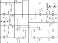
I have checked resistors around the input pair transistors - R14 (1.0k), R15 (33.2r), R16 (33.2r), R17 (392r) as well as R20 (1.0k), R21 (33.2r), R22 (33.2r), R23 (392r)
One anomaly, likely just me not understanding the annotation on schematics:
Both schematics I have located, show R17 and R23 as 392, which seems to be value code for a 3.9k resistor. However, checking resistors on the this channel and other channels, and the resistor color bands confirm 392r, with Orange - White - Red - Black - Brown (392r 1% color band code)
Would there be any other culprit of a high, unstable DC offset outside of the NPN, 2SC3381 (BL) and PNP, 2SA1349 (BL) dual BJT package transistors? Would the DC being negative point more towards the NPN transistor being faulty?
I know replacement transistors would be hard to find (originals anyways), and may have to resort to matching a quad of TO-92s
Would any of these be a satisfactory replacement, since I have them on hand?
Thanks for the assist. Attached is the datasheet and two schematics I have been working with, also used a GFA-7500 schematic, which matches up closely too.
But when I power up the Right amp channel, there is about (500)-(800)mV on start-up, then immediately drops down to ~(100)mV and then after a couple minutes slowly comes down to ~(33)mV. It stays at (33)mV with no change, I've set the bias (15mV) and no change to DC stays at (33)mV.
Other channels power on at ~50mV, and immediately drop to ~20mV and settle at <5mV - so something's not quite right, on the Right (channel)
I have checked resistors around the input pair transistors - R14 (1.0k), R15 (33.2r), R16 (33.2r), R17 (392r) as well as R20 (1.0k), R21 (33.2r), R22 (33.2r), R23 (392r)
One anomaly, likely just me not understanding the annotation on schematics:
Both schematics I have located, show R17 and R23 as 392, which seems to be value code for a 3.9k resistor. However, checking resistors on the this channel and other channels, and the resistor color bands confirm 392r, with Orange - White - Red - Black - Brown (392r 1% color band code)
Would there be any other culprit of a high, unstable DC offset outside of the NPN, 2SC3381 (BL) and PNP, 2SA1349 (BL) dual BJT package transistors? Would the DC being negative point more towards the NPN transistor being faulty?
I know replacement transistors would be hard to find (originals anyways), and may have to resort to matching a quad of TO-92s
Would any of these be a satisfactory replacement, since I have them on hand?
- BC547/BC557 (CBE pinout, 45Vce & Hfe 450-900)
- BC550/BC560 (CBE pinout, 45Vce & Hfe 200-450)
- KSC1845/KSA992 (ECB pinout, 120Vce & Hfe 300-600) --- I think this ECB pinout might be easier, but both can be made to work without too many pinout contortions
Thanks for the assist. Attached is the datasheet and two schematics I have been working with, also used a GFA-7500 schematic, which matches up closely too.
Attachments

Hi bullittstang,
The clarity of the jpg is much better than the pdf. Any chance of a zoom-out spanning R6 through R9 from the jpg source?
I would first capture some bias voltages. With black meter lead at ground, what are voltages at R6, the feedback node (junction of R9 and R24), voltage at C25-R24 node, and amp output at R9 ? Any DC voltage across R24 is evidence of leakage through C25; any voltage across R24 will contribute output offset amplified by ratio R6/R24 = ~28. You might be able to observe transient voltage across R24 if C25 leakage is the culprit.
Other defects are possibilities, but these measurements may suggest where to look next.
Good luck!
Sorry, but I can't, since I don't have the entire schematic in that version - I lifted that specific portion of the schematic someone else posted to an old thread here on DIYAudio.The clarity of the jpg is much better than the pdf. Any chance of a zoom-out spanning R6 through R9 from the jpg source?
I should have been more specific, but I replaced all the electrolytic capacitors with Panasonic EEU, specifically C25, C88 and C94/C95. So there shouldn't be any leakage across C25. I will check some voltages tonight, to see if it matches the schematic, but I can't find any out of spec resistors or diodes and it bias' fine. It is only having an issue with the DC offsetI would first capture some bias voltages. With black meter lead at ground, what are voltages at R6, the feedback node (junction of R9 and R24), voltage at C25-R24 node, and amp output at R9 ? Any DC voltage across R24 is evidence of leakage through C25; any voltage across R24 will contribute output offset amplified by ratio R6/R24 = ~28. You might be able to observe transient voltage across R24 if C25 leakage is the culprit.
With the bias measurements I mentioned, we should be able to estimate bias currents and gain insight to where the problem lies. 30mV offset isn't bad, but the settling behavior is suspicious. Maybe you can catch initial transient when behavior is most aberrant. input transistors are chief suspects. Bias current can often point the way.
Cold shot is a good exploratory tool. With a bit of practice, you can drip coolant almost drop-by-drop onto each suspect transistor. Compare with the good channel to develop a sense of what's normal behavior.
Cold shot is a good exploratory tool. With a bit of practice, you can drip coolant almost drop-by-drop onto each suspect transistor. Compare with the good channel to develop a sense of what's normal behavior.
Sorry for my poor technique below. I've noted measured voltages and derived bias currents.
The results look reasonable, so you may have to investigate these same measurement points during the turn-on transient while the misbehavior is more evident.
Note that there appears to be about 1mV across R24, but the accuracy may be questionable since you may be limited by the resolution of your DVM. Try measuring directly across R24, testing with both meter polarities to try confirming that the voltage drop is actually present, and not an artifact of subtracting two resolution-limited readings. If there were actually 0.56uA flowing, it would account for about 27mV of the offset seen at the output. But this error isn't very significant anyway.
But the 500mV to 800mV power-on offset is irksome, especially if it settles slowly in comparison with the other channel.
There are lots of possible culprits, including any of the four input transistors, C25, and other less probable defects. Because it's an easy test, I would try removing C25. Presence of C10 will keep the amp stable. If C25 is at fault, the amp will settle very quickly with good stability when it's removed. Of course you have to restore C25 for good low frequency performance.
Let us know what you experience. We can devise other troubleshooting experiments.
Good luck!
Thanks for the insights and suggestions @BSST
I decided to hook up a test speaker and see what the "actual" behavior is... not as bad as on the test bench. Not sure if that's because of grounding or the speaker load, but the "on" transient DC is 200mV and almost immediately drops to 35mV and settles out at 30mV within 30 seconds.
a lot better than 800mV I was seeing on the bench. I'm going to play some music and power cycle a few dozen times and see if there are any "nasty" noises from the speaker. Right now seems to be barely a cone movement inwards at power on and power off, which is tolerable to me.
Since I will be using this for the front stage of my HT for now, this channel might get moved to the LR or RR position in the chassis, so I have 3 more similar channels for the LCR positions.

Well it's all put back together in the chassis - I did switch RR with R channels, just in case there was any unwanted power on pop/noise.
Been listening for 30-45 mins and turned on/off 10+ times and strangely there is still -200mV intimal negative DC, but immediately drops to -40mV and settles at -32mV. But there is no annoying turn on pop or sound at all, even less than 12" from the speaker.
All I can hear is the "nuclear reactor" buzz/hum as the Transformer energizes all those caps and starts pulling 50-60 watts at idle, but even that goes down to a faint mechanical hum after 3 seconds. Can barely hear it with the top on and screwed down in a quiet room.
So, I'm going to listen to it and make a final judgement after a few days of break in. First impressions, no mistaking it's an Adcom amp, warm and punchy and very easy to listen to, not fatiguing at all. Seems to punch a little harder than 130watts - I would easily guess 150-175w into my 7.1r nominal speakers.
FYI - pain in the butt to put this beast back together. My meat cleaver hands barely fit to put the nuts on the speaker terminals and the wiring was challenging as well, but overall it is well built and the PCBs are extremely easy to work on, Never had to take the heatsink off, because it doesn't cover up the PCB like newer designed PCBs. Overall, impressed with the amp and think it was worth a couple days of work to clean, repair and upgrade.
- Home
- Amplifiers
- Solid State
- ADCOM GFA-7000 - High DC offset