I think "balanced" meaning equal output impedances, these impedances have to be seen from somewhere. When the emitter or the receiver have not a transformer, there is a need of biasing for the active circuits, usually half way of the power supply rails.
I don't call 'balanced' the input or the output of a single ended transformer. They are "floating" which means without any potential reference.
DANGER: Semantics ahead.
Last edited:
Hi Bob,
I have been using this a few times, and balanced the output impedances with an external Rout (like 100 ohms) on each output. I thought that in this setup I would have source common mode supression?
Jan
Hi Jan,
My definition of "source common mode rejection" for a balanced source is that the source, for all intents and purposes, acts very much like the floating winding of a transformer. In other words, it has little or no reference to ground. It has a largely undefined common mode voltage. A transformer with a center-tapped output with the center tap connected to ground violates this criteria. A true differential output amplifier with common mode feedback to define the output common mode voltage violates this criteria. A source that violates this criteria has the potential to create a ground loop depending on the nature of what type of receiver is at the other end. A source that meets this criteria can drive a single-ended load (one side connected to ground) with no problem.
If you have a balanced source that has high source common mode rejection, you can load it with a center-tapped resistance, and apply an external small signal to the center tap of that load resistance, and essentially no signal current will flow. The common mode output impedance of that source is very high. The THAT OutSmarts active balanced output driver satisfies this criteria.
This is a rather strict definition of a balanced source, and by this I do not mean to take a position that approaches failing this criteria are bad or not worthy of being described as balanced in the general less-formal consumer audio sense. In my VinylTrak preamplifier I implemented "balanced" outputs in the same way you described and most others do.
Cheers,
Bob
Hi Bob:
That was a good talk at BA2016 on the improved Hafler. With before and after measurements to boot! Any chance of showing pictures of the finished device? Whoever was filming forgot to move the camera up to the slides images at the end of your presentation!!!
mlloyd1
That was a good talk at BA2016 on the improved Hafler. With before and after measurements to boot! Any chance of showing pictures of the finished device? Whoever was filming forgot to move the camera up to the slides images at the end of your presentation!!!
mlloyd1
BTW I'm impressed by the noise spec on the SAE8300. Eight channels in a box, 4 stacked per side, each channel has a single PCB with PSU and amp all on the one board...and it achieves (if we take the manufacturer at his word) 128dB A weighted SNR. Perhaps the decision to go fully balanced, fully differential internally is driven by the pursuit of such low noise? And perhaps once designed, shedding the star ground leads to ease of manufacture and layout/wiring design especially for multichannel amps. (Bruno's designs also seem to have very impressive SNR stats.)
I should probably let you guys get back to discussing more complex issues...
Hi SGK,
That is quite a good number. We all have to be very careful in evaluating noise performance based on manufacturer's specs. There are 2 ways that S/N for a power amplifier are specified (apart from different weighting). The first is rms output noise voltage with respect to 2.83V rms (i.e., 1W @ 8 ohms).
The second is output noise voltage with respect to rms output voltage at rated power. The latter yields a better number, and is the one that the marketing department likes to use. The former is the one that John Atkinson of Stereophile uses. The former obviously compares two amplifiers on the basis of how noisy they are for a given set of loudspeakers.
I use this former definition, and I personally think it is the more honest definition. There will be those who disagree with me, of course, citing the matter of dynamic range. Dynamic range is not always the same as S/N. DANGER: Semantics ahead.
A 100w amplifier produces 28V rms at rated power. This is 20dB higher than 2.83V. The S/N of that amplifier will be 108dB by the former measure that John Atkinson quotes.
That having been said, 108dB A weighted wrt 2.83V is quite good, and many amplifiers out there do not do this well. At the same time, many of us routinely achieve this S/N with ordinary single-ended designs.
Looking at input-referred noise voltage is another way of stating the noise of a power amplifier on a somewhat level playing field. An amplifier that achieves input-referred noise of 10 nV/rt Hz is quite good. One that achieves 5 nV/rt Hz is very good.
A weighting makes the noise look better compared to un-weighted noise specifications, but the noise measurement bandwidth of the unweighted measurement is often not stated. Some state it for a 20kHz noise bandwidth, others use 80kHz, etc. White noise voltage generally goes up as the square root of noise measurement bandwidth.
If you want to look at only noise, as opposed to hum and noise, A weighting makes sense, as it strongly attenuates hum and some of its harmonics. The equivalent noise bandwidth ENBW of A weighting is about 13kHz. If you look at the A-weighted output noise voltage and divide it by SQRT 13,000, and then divide it by the voltage gain of the amplifier, you will get the input-referred input noise.
Cheers,
Bob
Hi Jan,
My definition of "source common mode rejection" for a balanced source is that the source, for all intents and purposes, acts very much like the floating winding of a transformer. In other words, it has little or no reference to ground. It has a largely undefined common mode voltage. A transformer with a center-tapped output with the center tap connected to ground violates this criteria. A true differential output amplifier with common mode feedback to define the output common mode voltage violates this criteria. A source that violates this criteria has the potential to create a ground loop depending on the nature of what type of receiver is at the other end. A source that meets this criteria can drive a single-ended load (one side connected to ground) with no problem.
If you have a balanced source that has high source common mode rejection, you can load it with a center-tapped resistance, and apply an external small signal to the center tap of that load resistance, and essentially no signal current will flow. The common mode output impedance of that source is very high. The THAT OutSmarts active balanced output driver satisfies this criteria.
This is a rather strict definition of a balanced source, and by this I do not mean to take a position that approaches failing this criteria are bad or not worthy of being described as balanced in the general less-formal consumer audio sense. In my VinylTrak preamplifier I implemented "balanced" outputs in the same way you described and most others do.
Cheers,
Bob
Got it. In my case it worked because the receiver was a differential amplifier with no ground reference on the inputs.
Jan
That is a beautiful amplifier. 300wpc @ 8 ohms X 8. 128 pounds!! Holy cow!!
It is nicely spec'd. They say explicitly that noise is wrt rated output. They also say 30 uV A weighted at the output, and gain = 28.
<0.05% up to 20kHz is not great, but who knows how much margin they are using.
Cheers,
Bob
Bob, I took to heart the advice in post #7526 and started simulating the 2T shunt feedback current source in the frequency domain, studying gain and phase. The simulation results seem to be telling meI made a plot of simulated phase margin vs. stray capacitance, image #3 below. As you can see, phase margin crosses zero when Cstray is above 8 picofarads. That's scary!
- Self inductance of the transistor pins (up to 15 nH) doesn't make much difference. I didn't study mutual inductance however.
- The impedance of the load driven by the current source is critical. Lower impedance loads (such as the emitters of an LTP) result in MUCH worse phase margin.
- The ratio of currents between the two transistors doesn't make much difference. I froze it at ten to one so you wouldn't gripe.
- Stray capacitance across the current sense resistor ("R1" in the schematic below) can destroy phase margin.
- Different transistor part#s (i.e. different SPICE model parameters) gave different amounts of phase margin. The Fairchild KSA992 (model supplied by Linear Technology) was worst among the PNPs I tried. The BC560C (model supplied by Cordell Audio) was second worst; it needed 30pF of stray cap to begin oscillating.
To get the transient simulation results in image #2, I used the LTSPICE directive ".IC" (Initial Conditions) to nudge the simulated circuit away from its metastable state. The LTSPICE deck (.asc file) is attached if anybody wants to horse around with it.
I myself have decided to stop using this particular topology to implement a current source; I've gone to (VREF-VBE)/R circuits, with and without cascode. Mostly, with cascode.
Hi Mark,
Thanks for doing this. I'll try some of the sims when I get a chance. You make some good points. Your use of a 13-ohm load is pretty low, but you could argue that the load looking into the emitters of an un-degenerated LTP might be that low if each transistor was running at 1mA, and perhaps even somewhat inductive, depending on what the bases are connected to.
Out of concern for HF EMI effects in the common mode, I almost always in practice put a 1k resistor between the tail of the LTP and the current source, so that may be helping me as well.
What method did you use to evaluate loop gain?
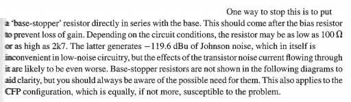
As stated earlier, placing a 100 ohm resistor in the base of the reference transistor should clean all of this up (no capacitor need be added). Putting in such a stopper resistor is no big deal. I would keep using this current source where it seems like a good solution. I will definitely address this stability issue in the second edition.
Cheers,
Bob
128dB (A weighted) S to N ref 300W into 8ohms with a gain of +28dB gives an A weighted Ein of 5.2nV/rtHz
30uVac of A weighted output noise is equivalent to A weighted Ein of 8.1nV/rtHz
If you add on 4dB (1.58 times), to convert A weighting to flat, you end up with 8.2nV/rtHz and 13nV/rtHz Both are pretty good, but not exceptional.
To compare 128dB s/n for 300W to R.Cordell's preferred ref of 1W you end up at 103.2dB A weighted s/n ref 1W and if one adds on 4dB one ends up at ~ 99dB s/n ref 1W
The conversion from Aweighting to flat depneds very much on the proportions of HF noise and LF noise in the total noise figure of a band limited 10Hz to 100kHz "flat" measurement. The conversion to Aweighting could take off as little as 2dB or as much as 6dB. I took 4dB in my example as an average.
Last edited:
Speaking about balanced outputs, two interesting circuits :
(source Pro Audio Design Forum • View topic - Balanced Outputs )
designed by Barry Porter

designed by Graeme John Cohen

(source Pro Audio Design Forum • View topic - Balanced Outputs )
designed by Barry Porter
designed by Graeme John Cohen
As stated earlier, placing a 100 ohm resistor in the base of the reference transistor should clean all of this up (no capacitor need be added). Putting in such a stopper resistor is no big deal.
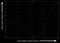
I predict that when you simulate this 2T circuit using the BC560C SPICE model from Cordell Audio's website, you will find that 100R in series with the base makes the phase margin worse instead of better. I predict you will find yourself in agreement with Douglas Self, that sometimes this resistor needs to be as large as 2.7K to be effective. LTSPICE's feature that allows you to make a plot of stepped parameter (X axis) vs .MEASured quantity (Y axis), will give you a graph of Rseries versus PhaseMargin ... same as my image#3 that graphs Cstray versus PhaseMargin. Phase Margin gets worse before it gets better. Really.
Perhaps you might agree with the claim that some audio DIYers employ the "Monkey See, Monkey Do" approach to circuit design. So it would be nice if an influential book like your 2nd edition, contains schematics with current sources that don't oscillate. Then mindless copiers will have a better chance of success.
Hi Bob:
That was a good talk at BA2016 on the improved Hafler. With before and after measurements to boot! Any chance of showing pictures of the finished device? Whoever was filming forgot to move the camera up to the slides images at the end of your presentation!!!
mlloyd1
Thanks! Unfortunately I was so squeezed on time to complete the project that it never made it past the single-channel perf board-on-heatsink stage.
Cheers,
Bob
Hi Richard,
I'd like to say that you've exposed the secret for extreme insensitivity to external noise with driven guards and another level of shielding. You're talking about normal practice in research and calibration labs. Application in the consumer area might be a tough go for the increased cost. It might actually really help in phono applications, and in the preamp to amp signal run.
-Chris
I predict that when you simulate this 2T circuit using the BC560C SPICE model from Cordell Audio's website, you will find that 100R in series with the base makes the phase margin worse instead of better. I predict you will find yourself in agreement with Douglas Self, that sometimes this resistor needs to be as large as 2.7K to be effective. LTSPICE's feature that allows you to make a plot of stepped parameter (X axis) vs .MEASured quantity (Y axis), will give you a graph of Rseries versus PhaseMargin ... same as my image#3 that graphs Cstray versus PhaseMargin. Phase Margin gets worse before it gets better. Really.
Perhaps you might agree with the claim that some audio DIYers employ the "Monkey See, Monkey Do" approach to circuit design. So it would be nice if an influential book like your 2nd edition, contains schematics with current sources that don't oscillate. Then mindless copiers will have a better chance of success.
Hi Mark,
I assure you, I will definitely discuss this issue in the second edition.
Where did you find that statement from Doug about the base resistor value? Can you give me the page number and what edition of his power amp book it is in?
How did you measure the phase margin?
Cheers,
Bob
Bob, I just used the bog standard procedure for making open loop Bode plots. I am sure you did exact same thing when you simulated Figure 9.7 (p.181) in the first edition of your book.I've attached a representative plot of phase margin versus 2T current source "base stopper" resistance. Not all transistor types (i.e. SPICE models) display this behavior in simulation, but many do. Phase margin gets worse before it gets better. 100 ohms is a particularly disastrous choice.
D. Self mentions 2.7Kohm base stoppers on page 72 of the 1st edition of his Small Signal Audio Design book, excerpt below.
- Identify the complete loop
- Find a convenient place to break the loop
- Drive an AC test signal at the "input" of the broken loop
- Observe the signal at the "output" of the broken loop
- Plot magnitude and phase of V(out)/V(in)
- Use LTSPICE ".MEAS" statements to read Phase Margin off the plots
D. Self mentions 2.7Kohm base stoppers on page 72 of the 1st edition of his Small Signal Audio Design book, excerpt below.
Attachments
That is not correct. You drive the opened loop with a zero impedance source and
measure the output without load. But in reality, the input is driven by the impedance
of the output and the output is loaded by the input.
There is a loop gain probe somewhere in the LTspice examples.
I will try that myself over the season.
For measured s-parameters, the exact equation for the self-terminated loop is
G = (S21 - S12) / (1 - S11*S22 + S21*S12 -2 * S12) ( Randall/Hock equation )
Rhea writes in his oscillator book that you can open the loop even
inside the resonator and the outcome is still OK.
regards, Gerhard
ps.
< https://www.amazon.de/Discrete-Osci...r=1-2&keywords=Randall+W.+Rhea+++Artech+house >
There was a older oscillator book by Rhea that does not carry it.
Last edited:
Fortunately the 2T current source contains a (very) low impedance output which drives a (moderately) high impedance input. So if your simulation assistant decides to break the loop right there, between those two elements, loading errors are small. And if she decides to break the loop by simply splicing a zero-Thevenin-resistance independent voltage source (DC value = zero, AC value = one) in series between those two elements, loading errors are very small. Much smaller than the errors introduced by pretending the SPICE model of a BC560C or KSA992 is anywhere close to accurate when simulating 78 Megahertz oscillations (post #7585, image 2).
- Home
- Amplifiers
- Solid State
- Bob Cordell's Power amplifier book