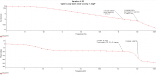
Phase Margin = (180 deg - OL Phase) at the frequency where the open-loop gain drops to the closed-loop gain level.
For unity-gain amps, this happens to be zero dB. For your amp, this is 20.8 dB, shown in your 3rd plot. Quick calculation would give CL gain = 1/feedback = (330+30)/30 = 11 = 20.8 dB. You want at least 60deg of PM. It is common to define "loop gain" with is the OL gain * feedback ratio. Then you can reference to 0 dB, just like with unity gain.
Gain Margin ((1/feedback)/OL Gain) at the frequency where the OL Phase = 180deg.
In dB, just subtact the OL gain from the low frequency CL gain where OL phase=180 deg.
With 1/feedback you mean 1/(Aol-Acl) correct?
And instead of making sure that in the openloop plot PM>180 at 0dB we want PM>60 at Aol=Acl=20.8dB?
Its unclear to me what the difference is between the Aol of the amp and the Aol of the loop itself. I merely know Aol and Acl of the amplifier. But what you are saying is that the Aol gain of the loop is the point where openloop gain of the amplifier is equal to the Acl of the amplifier?
In class this subject confused me too, hence me mixing up some rules of thumb. Though I passed the control theory exam anyhow lol.
With 1/feedback you mean 1/(Aol-Acl) correct? <edit> Its unclear to me what the difference is between the Aol of the amp and the Aol of the loop itself. I merely know Aol and Acl of the amplifier. But what you are saying is that the Aol gain of the loop is the point where openloop gain of the amplifier is equal to the Acl of the amplifier?
For stability analysis of a differential amp, it is probably easiest to look at each side as a separate amplifier.
- Aol = Voutp/(Vinp-Vinm) = -Voutm/(Vinp-Vinm)
- feedback (aka beta) = Re/(Rf+Re) <-- simply the voltage divider of your feedback resistors.
- Aloop = beta*Aol
- Acl = Aol/(1 + beta*Aol)
And instead of making sure that in the openloop plot PM>180 at 0dB we want PM>60 at Aol=Acl=20.8dB?
Close but not quite. Phase margin is not equal to phase.
Phase margin is how far above 180 deg the phase is when Aloop = 1 (0 dB).
Gain margin is how far Aloop is below 0 dB when the phase = 180 deg.
What exactly are we checking here? We are checking that the denominator of the Acl equation does not go to zero. If it does, then the gain approaches infinity, and an oscillator is born.
(1 + beta*Aol) not= 0
When |beta*Aol| = 1, and its phase = 180 deg, then (1 + beta*Aol) = (1 - 1) = 0. This is like crossing the beams in Ghostbusters.
Correct on phase margin, I believe, but incorrect on gain margin.
Your gain margin would be 11/2.08 = 5.29 = 14.5 dB. (which is a good GM)
Your gain margin would be 11/2.08 = 5.29 = 14.5 dB. (which is a good GM)
iteration 4.94
Okay apparently i'm still not getting gain margin. However, stable is stable, testing with large squarewaves and tweaking Ccomp works too 😀.
I just discovered that giving the output stage more current gain and eliminating the TIP41 pre output driver greatly reduces distortion. Using an extra set of NJW's THD is downto 0.005% at 20kHz at 100W. Now I can even push it to 109W without clipping and matching the NJW's should be a little less critical. Looks really great.
Though this comes at the expanse of speed, a lot of speed. Using both the TIP41 predriver and 2 sets of NJW's regains this speed but requires more Ccomp, resulting a bit more THD (0.008%).
Step responses are added below. Both are using 2 sets of NJW's per side. I gravitate more towards the slower version, without the TIP41 predriver. Slewrate is merely an indication of bandwidth capability right?
Cheers and happy easter,
Ruben
Attachments
I would go with the faster version that gives you 31 V/us slew rate. 11 V/us is too close to your minimum required slew rate. Getting the distortion lower with the extra output transistors is probably just a matter of re-tuning the bias current. BTW, you don't need to make the ballast resistors so large. 0.22 ohms is plenty.
Bandwidth is a small signal characteristic, and slew rate is a large signal characteristic. Amps with low SR can have high BW, and vice versa, but they usually correlate.
Bandwidth is a small signal characteristic, and slew rate is a large signal characteristic. Amps with low SR can have high BW, and vice versa, but they usually correlate.
DB140/139 really this good?
Hi all,
Though being really happy with the design so far i've still been trying to eliminate the pre output emitter follower. I just tried some substitutes for the TIP40/41's and found that the DB140/DB139 allows for great speed while maintaining good stability. The step response is much much cleaner now, so much so that I don't quite trust the spice model. However the spice model does not look less detailed to me.
It now swings the complete voltage range within 1us and THD is downto 0.005%. Too good to be true? Once again I attached some plots. Note the HF hump in the closedloop gain, though openloop plot does show good stability if i'm correct. Schematics stuffed with probes are included. One at idle, the other at 100W into 4 ohms. I won't be surprised if there's some issue i am overlooking.
The output transistors are now biased such that with a 4 ohm load, idling and at full blast they dissipate almost the same (only 600mW more). This should reduce the chance of thermal runaway to silicone heaven.
Any tips for over-current protection circuits? I'm thinking of using a 'high side current monitor', some latch and a relay.
All thoughts and opinions would be greatly appreciated.
Cheers,
Ruben
Attachments
Looking good.
I don't see any red flags. Build it.
After you build it, if the current in your output transistors is not stable with temperature, you may want to experiment with the emitter resistor values in your driver and pre-driver stages.
I don't see any red flags. Build it.
After you build it, if the current in your output transistors is not stable with temperature, you may want to experiment with the emitter resistor values in your driver and pre-driver stages.
Toys are here!
Hi All,
It took a little while before I got to ordering parts. Now most of them are here so I can start breadboarding soon. Yet to order a nice resistor kit, maybe Velleman carbon films.
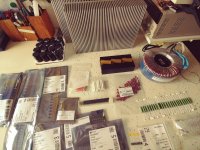
IB Fluck located in Germany kindly sent me samples of multiple Linear Systems dual JFets, Absolutely great company and great parts. I got a bunch of PP film caps and landed on 0.1 ohm emitter resistors for now.
This will be the most complex circuit I have put on the breadboard so far, hopefully spitting up in parts will help. To reduce errors, I might just have a prototype pcb done with sockets so I could swap some resistors. Do projects go this route more often? I'm certainly tempted to go PCB right away, which would also allow me to tab and drill the heatsinks just once and test the output trannies in their final position. Surely this ride will not be that smooth haha.
Let me know what you think. I'm sure you all have been here many times before.
Cheers,
Ruben
Hi All,
It took a little while before I got to ordering parts. Now most of them are here so I can start breadboarding soon. Yet to order a nice resistor kit, maybe Velleman carbon films.

IB Fluck located in Germany kindly sent me samples of multiple Linear Systems dual JFets, Absolutely great company and great parts. I got a bunch of PP film caps and landed on 0.1 ohm emitter resistors for now.
This will be the most complex circuit I have put on the breadboard so far, hopefully spitting up in parts will help. To reduce errors, I might just have a prototype pcb done with sockets so I could swap some resistors. Do projects go this route more often? I'm certainly tempted to go PCB right away, which would also allow me to tab and drill the heatsinks just once and test the output trannies in their final position. Surely this ride will not be that smooth haha.
Let me know what you think. I'm sure you all have been here many times before.
Cheers,
Ruben
PCB design
Dear audio enthousiasts,
If I would test it on PCB, it would look something like this:
Front:
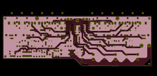
Back:
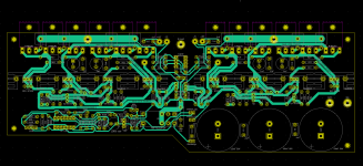
This is my first power amp PCB so I'm sure there's much room for improvement and I hope some of you may point this out to me.
Note that the supply current will pass the frontend before it reaches the output stages, rather than the other way round. Would it be desirable to connect the Vcc connection to the top via a jumper and place the star ground on the bottom? This way current arrives at the output stage first.
It's using a place for Vcc and a ground 'spider'. Any do's and don'ts concerning star grounds that I'm missing? I also ended up including temperature protection.
Temperature protection, CMFB and power section:
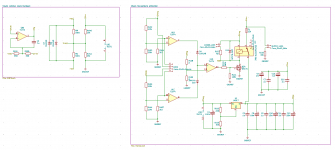
Amplifier schematic:
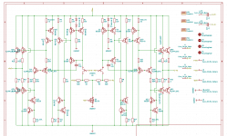
I might do another PCB where the safety circuits and capacitor bank are located on their own PCB which would be mounted on top of the amplifier board. A two storied pcb so to speak to allow for more total board space. Since I have two giant heatsinks I could go one per channel, giving me twice the board space, though this would make the amp insanely big and heavy, maybe too big for me.
All of your thoughts and opinions are most welcome!
Cheers and all the best to you all,
Ruben
Dear audio enthousiasts,
If I would test it on PCB, it would look something like this:
Front:

Back:

This is my first power amp PCB so I'm sure there's much room for improvement and I hope some of you may point this out to me.
Note that the supply current will pass the frontend before it reaches the output stages, rather than the other way round. Would it be desirable to connect the Vcc connection to the top via a jumper and place the star ground on the bottom? This way current arrives at the output stage first.
It's using a place for Vcc and a ground 'spider'. Any do's and don'ts concerning star grounds that I'm missing? I also ended up including temperature protection.
Temperature protection, CMFB and power section:

Amplifier schematic:

I might do another PCB where the safety circuits and capacitor bank are located on their own PCB which would be mounted on top of the amplifier board. A two storied pcb so to speak to allow for more total board space. Since I have two giant heatsinks I could go one per channel, giving me twice the board space, though this would make the amp insanely big and heavy, maybe too big for me.
All of your thoughts and opinions are most welcome!
Cheers and all the best to you all,
Ruben
Attachments
Looks good, Ruben.
I once built a 400W amplifier on a protoboard, and then copied it to a soldered breadboard. That amplifier got me my first job as an audio design engineer.
I once built a 400W amplifier on a protoboard, and then copied it to a soldered breadboard. That amplifier got me my first job as an audio design engineer.
Hi Russel,
Good to hear, hope the tracks are laid down decently. I got a tip to make it a 4 layer pcb with Inner V+ and GND planes and two outer signal layers. This would allow for much thicker tracks but at 4 times the cost.
That 400W amp must've been a great design. Did you show it to somebody within the field you already knew?
Cheers,
Ruben
CMFB Verified!
Simplified front end is tested and the common mode feedback is verified. The summing integrator does the job nicely. This is simply the Njfet diffpair and pnp voltage followers. No active loads or global feedback yet. I did need to use a trimmer to get rid of the offset between the collectors.
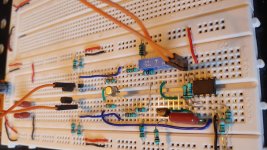
I discovered that when using the integrator CMFB I need to tie 'signal source ground' to the ground of the bench supply via a capacitor, whether im using capacitors between the signal source and the jfet gates or not.
However, when using a simple jfet current source (no CMFB) I can leave the grounds unconnected. I have no idea why I need a capacitor between the grounds in one situation but dont need it in the other. Any ideas? Is this really peculiar or is it just me?
As signal source im using the function generator of a NI myDAQ which is powered by usb by a laptop. The osciloscope im using is accomadated by the same device.
Much cheers,
Ruben
Simplified front end is tested and the common mode feedback is verified. The summing integrator does the job nicely. This is simply the Njfet diffpair and pnp voltage followers. No active loads or global feedback yet. I did need to use a trimmer to get rid of the offset between the collectors.

I discovered that when using the integrator CMFB I need to tie 'signal source ground' to the ground of the bench supply via a capacitor, whether im using capacitors between the signal source and the jfet gates or not.
However, when using a simple jfet current source (no CMFB) I can leave the grounds unconnected. I have no idea why I need a capacitor between the grounds in one situation but dont need it in the other. Any ideas? Is this really peculiar or is it just me?
As signal source im using the function generator of a NI myDAQ which is powered by usb by a laptop. The osciloscope im using is accomadated by the same device.
Much cheers,
Ruben
Darlington Diamond Class A Bias
Dear All,
Since I have power components to accommodate much more dissipation, class A has always been in the back of my mind. The elegance of the diamondlike buffer kept me away from more bias current until I realized darlington prebuffers should push it into class A. And ohh yes... it does.
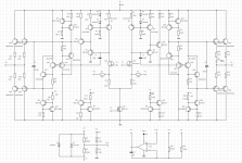
For class A it is still rather efficient at about 30 percent. However with simulated distortion levels being below audible anyway, I'm not sure if burning off a stupid 370Wats idling is worth it. Fourier gave 0.0018% in class AB, 0.0009% in class A. Bandwidth is better too, which was plenty good in class AB anyhow.
I'm excited to find out if my ears can pick up any other differences. Simulation results driving a 4 ohm resistive load are added below.
Big cheers,
Ruben
Dear All,
Since I have power components to accommodate much more dissipation, class A has always been in the back of my mind. The elegance of the diamondlike buffer kept me away from more bias current until I realized darlington prebuffers should push it into class A. And ohh yes... it does.

For class A it is still rather efficient at about 30 percent. However with simulated distortion levels being below audible anyway, I'm not sure if burning off a stupid 370Wats idling is worth it. Fourier gave 0.0018% in class AB, 0.0009% in class A. Bandwidth is better too, which was plenty good in class AB anyhow.
I'm excited to find out if my ears can pick up any other differences. Simulation results driving a 4 ohm resistive load are added below.
Big cheers,
Ruben
Attachments
When driving 4 ohm at 100W at 20k Hz that isFourier gave 0.0018% in class AB, 0.0009% in class A.
- Home
- Amplifiers
- Solid State
- Class AB diff-amp design
