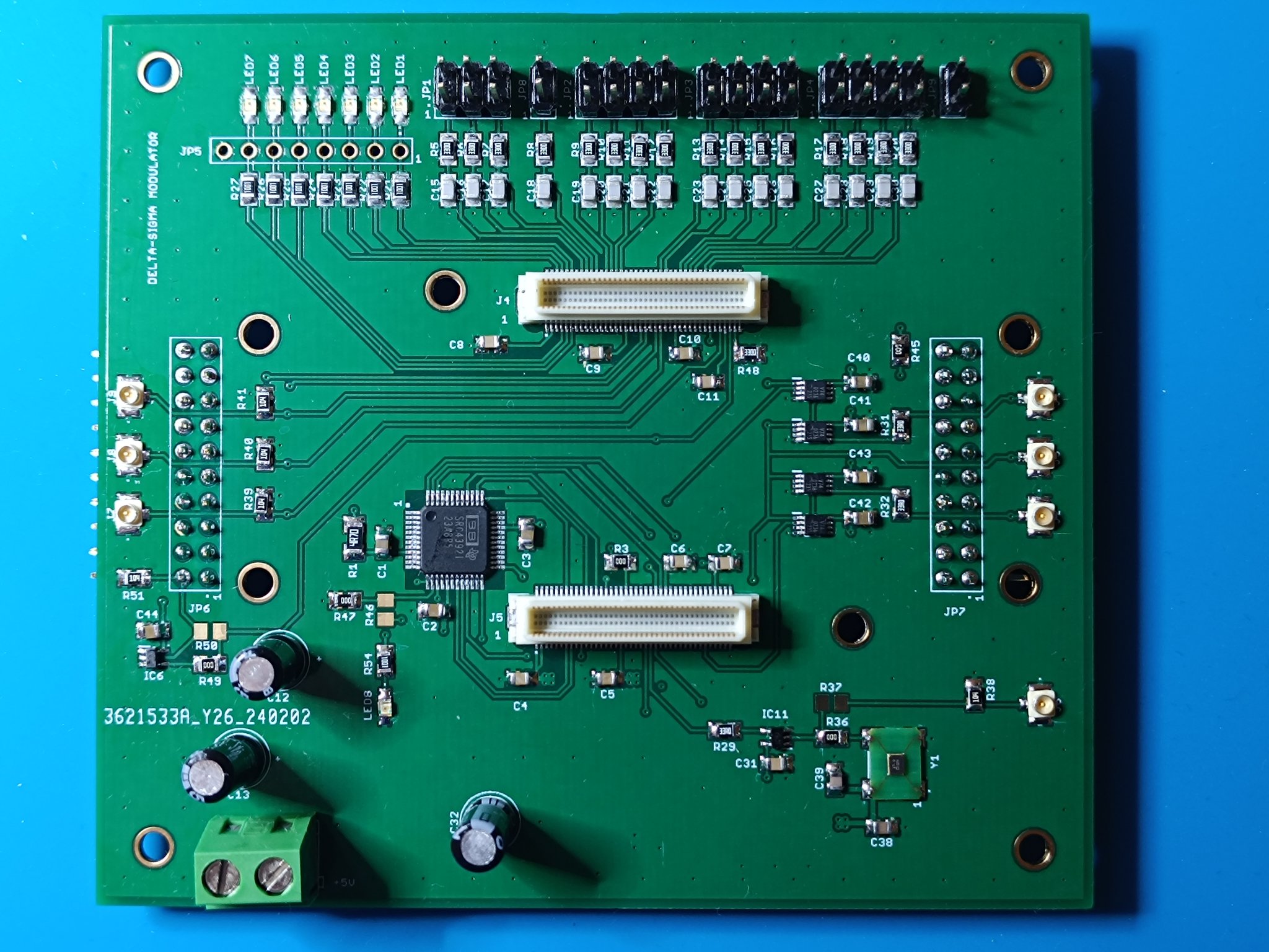
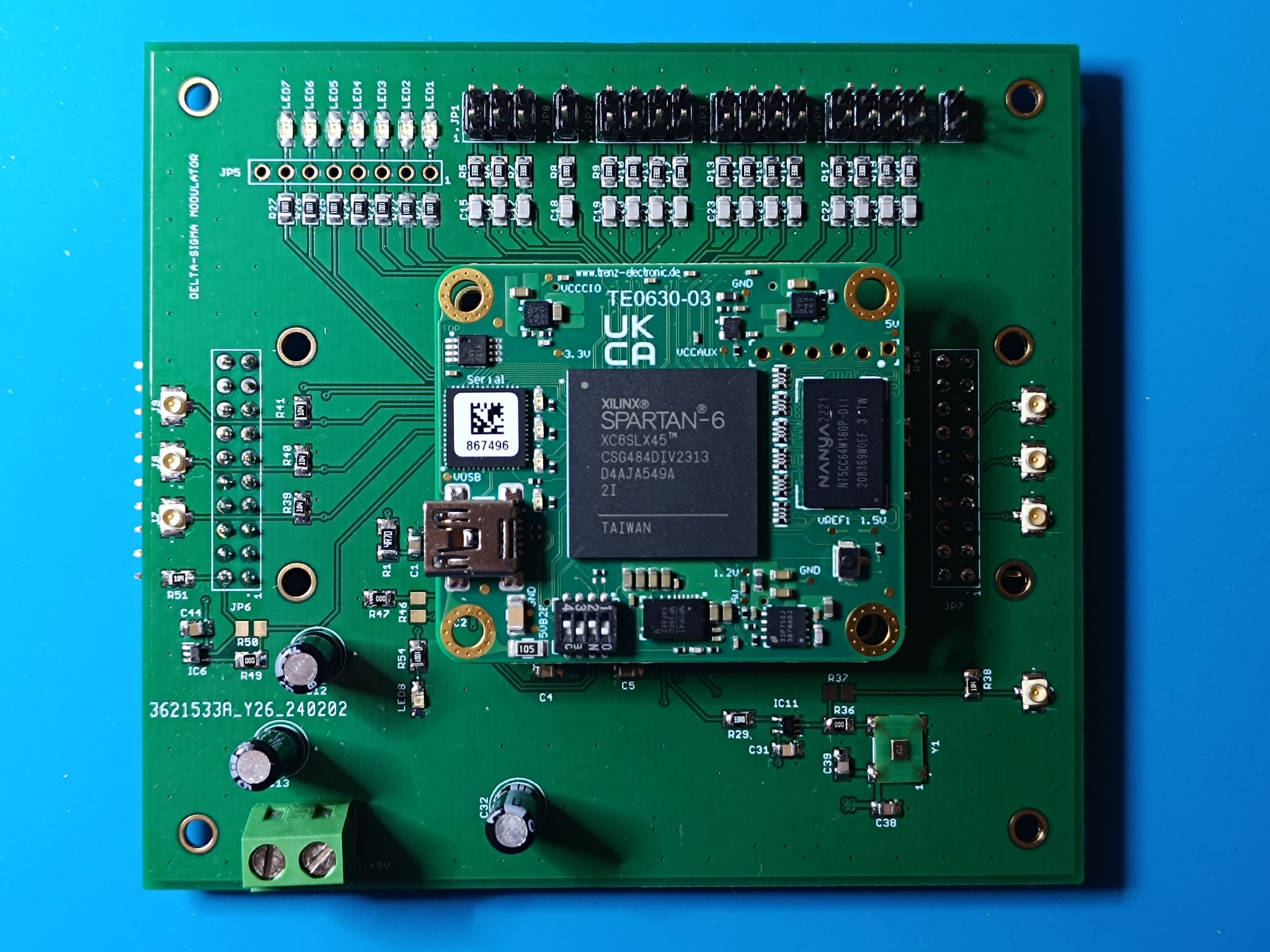
Hi all,
I made a separate PCB for the Delta Sigma Modulator by MarcelvdG shown in the
https://www.diyaudio.com/community/threads/valve-dac-from-linear-audio-volume-13.308860/
Thanks to Marcel for this project.
It is intended for Trenz TE0630 LX45 and LX75 FPGA modules.
This module is easy to program via USB and the Trenz application:
https://wiki.trenz-electronic.de/pages/viewpage.action?pageId=10620253
This module must be configured by shorting R102 pads on the FPGA board.
Actual LX45 configuration file see:
https://www.diyaudio.com/community/...r-audio-volume-13.308860/page-76#post-6569767
Actual LX75 configuration file see:
https://linearaudio.net/sites/linearaudio.net/files/additionaldatavalveDACversion2p1.zip
The FPGA code contains a sigma-delta modulator that has three modes selectable by switches.
Similarly, we can choose a filter.
You can read a lot of information about this modulator in the document:
https://linearaudio.net/sites/linearaudio.net/files/03 Didden LA V13 mvdg.pdf
Additionally, I included some information in the schematic.
This version has only I2S input/output.


I put schematic, boom and gerber files.
I made a separate PCB for the Delta Sigma Modulator by MarcelvdG shown in the
https://www.diyaudio.com/community/threads/valve-dac-from-linear-audio-volume-13.308860/
Thanks to Marcel for this project.
It is intended for Trenz TE0630 LX45 and LX75 FPGA modules.
This module is easy to program via USB and the Trenz application:
https://wiki.trenz-electronic.de/pages/viewpage.action?pageId=10620253
This module must be configured by shorting R102 pads on the FPGA board.
Actual LX45 configuration file see:
https://www.diyaudio.com/community/...r-audio-volume-13.308860/page-76#post-6569767
Actual LX75 configuration file see:
https://linearaudio.net/sites/linearaudio.net/files/additionaldatavalveDACversion2p1.zip
The FPGA code contains a sigma-delta modulator that has three modes selectable by switches.
Similarly, we can choose a filter.
You can read a lot of information about this modulator in the document:
https://linearaudio.net/sites/linearaudio.net/files/03 Didden LA V13 mvdg.pdf
Additionally, I included some information in the schematic.
This version has only I2S input/output.
I put schematic, boom and gerber files.
Attachments
Last edited:
Can you give me the working conditions of this FPGA? For example, the working power supply, working current, and how many Mhz the clock uses? I can redo the FPGA circuit board. The reason I redo the PCB is because I can't buy an FPGA module. I want to know the relevant information. I have been paying attention to this modulator for a long time. I will also make public the schematic diagram and the complete information of the PCB
Why not? Trenz has them in stock, but with a different type number because of some minor redesigns. They also added a logo to facilitate export to the UK. Are you in a country Trenz can't export to, but Xilinx can?
https://shop.trenz-electronic.de/de...LX45-2I-128-MByte-DDR3L-Mini-USB-2.0-4-x-5-cm
https://wiki.trenz-electronic.de/plugins/servlet/mobile?contentId=195205776#content/view/195205776
https://shop.trenz-electronic.de/de...LX45-2I-128-MByte-DDR3L-Mini-USB-2.0-4-x-5-cm
https://wiki.trenz-electronic.de/plugins/servlet/mobile?contentId=195205776#content/view/195205776
It's this module, it's expensive, it's hard to buy a module, and now it's less than $40 for a single FPGA chip, and if you buy a module alone, it's more than $40. Plus JLCPCB I use a 6-layer board here to make a free proof, I just want to know how much mA is the complete power consumption of the FPGA, how many mA, how many power supplies, how many mA, I want to make an SDM modulator,,,
Ah, it's too expensive. Fair enough.
Besides an FPGA, the module also contains DC-DC converters, configuration memory, two crystal oscillators of which one is used during start-up (the 24 MHz one), a DRAM that isn't needed for this modulator and a USB interface (not used for the modulator, but can apparently be used for programming the configuration memory if you don't do that with a JTAG interface).
The main supplies are 1.2 V and 3.3 V. The core runs off the 1.2 V and I have all the I/Os running off the 3.3 V. The module schematics are on the Trenz website, by the way. The module's DC-DC converters generate the 1.2 V and 3.3 V from a 5 V module input. There are also 1.5 V and 2.5 V supplies, but the 1.5 V is for the DRAM that isn't needed and the 2.5 V isn't used at all.
The only information I have about the currents is the current going into the 5 V input of the module:
https://www.diyaudio.com/community/threads/valve-dac-from-linear-audio-volume-13.308860/
"three hundred something milliamps from the 5 V supply the last time I measured it. As this was several configuration file updates ago and as the current drawn from the 5 V supply can change when the configuration file is changed, I recommend counting on 700 mA from the 5 V supply."
Most of that must be used in the core, so you have to multiply it by four to get an estimate of the 1.2 V supply current.
Last edited:
Actually, it could be that some of the switches are connected to an I/O bank that is supplied by the 2.5 V. Those might as well use 3.3 V, though.
Regarding clocks, besides the 24 MHz oscillator on the module that's used during start-up, there is a 27 MHz crystal oscillator on the main PCB that's used for the audio processing. Inside the FPGA, it's converted to a 189 MHz (version 3) or 216 MHz (version 2.1) clock frequency for the FIR filters and several other frequencies for SPI and I2S interfaces.
Regarding clocks, besides the 24 MHz oscillator on the module that's used during start-up, there is a 27 MHz crystal oscillator on the main PCB that's used for the audio processing. Inside the FPGA, it's converted to a 189 MHz (version 3) or 216 MHz (version 2.1) clock frequency for the FIR filters and several other frequencies for SPI and I2S interfaces.
Last edited:
Ok, thank you very much for your reply, gave me the relevant information, there are only two working power supplies, as for the 5V voltage, what is the current mA, I don't care, I know that FPGA has better LDO, so that I can try to do discrete DSD decoding when I have time, I also read a lot of your topics and learned a lot of related knowledge,
Last edited:
I'm not sure if you did or didn't understand the last sentence of post #8, but in case you didn't: the DC-DC converters on the FPGA module have an efficiency less than 100 %, so the power drawn from the 1.2 V must be smaller than the power going in via the 5 V input. For example, when the current the FPGA module draws from the 5 V is 360 mA, the power going in is 1.8 W, so the current drawn from the 1.2 V must be less than 1.5 A. I would count on 2.5 A or so because the measurement was done with an old configuration file.
Actually, it's better to test the working current of the new version of the profile, so it's more straightforward, are you sure that 2.5V is not in the working power supply? It's definitely 1.2 and 3.3V working, so I can find two low-noise LDOs instead of DC-DC, and the FPGA's flash isn't working? Does EEPROM store configuration files?
I looked at my constraints file and found that I've put everything on LVCMOS33 except two inputs that read DIL-switch settings on the FPGA module, signals lampsoff and lampenknop. Those have no I/O standard specified, which according to the Xilinx documentation (UG381 page 22) means they are LVCMOS25 inputs and use VCCAUX (table 1-5, UG381 page 39). I couldn't use 3.3 V for these inputs because they are in I/O bank 1, which gets a 1.5 V supply on the TE0630 modules (because it interfaces with the 1.5 V RAM that isn't needed).
All in all, in order to avoid needing 2.5 V, one would have to modify the .ucf file, add that these two inputs have to be LVCMOS33 and rerun synthesis and implementation.
All in all, in order to avoid needing 2.5 V, one would have to modify the .ucf file, add that these two inputs have to be LVCMOS33 and rerun synthesis and implementation.
Thank you for providing detailed information, but I also have no knowledge of FPGA SDM and I am unlikely to modify the constraint file. I am also constantly exploring the process of digital circuits. Can you modify an LX45 filter frequency of 180MHz+to provide a dedicated configuration file for relevant DIY enthusiasts?,
However, I also contacted someone who is working on signal processing to try out FPGA IO issues and power supply issues
He gives me the feeling that there is not a high chance of him being able to do it. I still want someone like you with relevant knowledge to create an exclusive configuration file, which will be much better
It would make more sense for more people if the FPGA firmware was written to accommodate standard audio clock frequencies. I understand the reason for using 27MHz, but there are no very low phase noise clocks available at that frequency. I would love to try to PWM algorithm but just won't work as is to compete with the high quality reproduction I can get with Iancanada, Andrea Mori, and or Acko Labs ultra low phase noise clocks.
The LX45 version is the same as your previous V3, the same frequency,
That's correct. Version 1, version 2 (which has a serious bug) and version 2.1 (bugfix) are meant for Trenz TE0630 LX75 modules and version 3 for LX45 modules.
- Home
- Source & Line
- Digital Line Level
- Delta Sigma Modulator by MarcelvdG