Well you can cascade them, and that’s fun (tho not at all power efficient).
Also HP use a diamond buffer in the output for the 3325A signal generator. Dunno when it was designed, but the first edition of the manual is ‘78.
Also HP use a diamond buffer in the output for the 3325A signal generator. Dunno when it was designed, but the first edition of the manual is ‘78.
Attachments


Member
Joined 2009
Paid Member
Wow, that’s a lot of parts, but maybe the cascode takes the ‘heat’ off the outputs, brings thermal stability ?
Wow, that’s a lot of parts, but maybe the cascode takes the ‘heat’ off the outputs, brings thermal stability ?
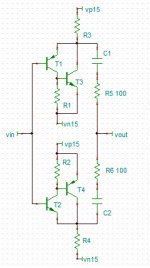
It’s a cascade, not cascode. The idea is to use a large quantity of inexpensive transistors to spread the dissipation across multiple devices, achieving wide bandwidth and low distortion into moderate tweeter and small full-range type loads.
It works quite well. I use it in my ‘noiseunit’ active 2-way speakers, with a 5W and 15W nominal output stage:
https://www.diyaudio.com/forums/mul...ssion-line-computer-speakers.html#post5389974
There’s a thread on the topology:
https://www.diyaudio.com/forums/sol...eap-low-thd-10w-amp-tip41c-4.html#post5307265
Member
Joined 2009
Paid Member
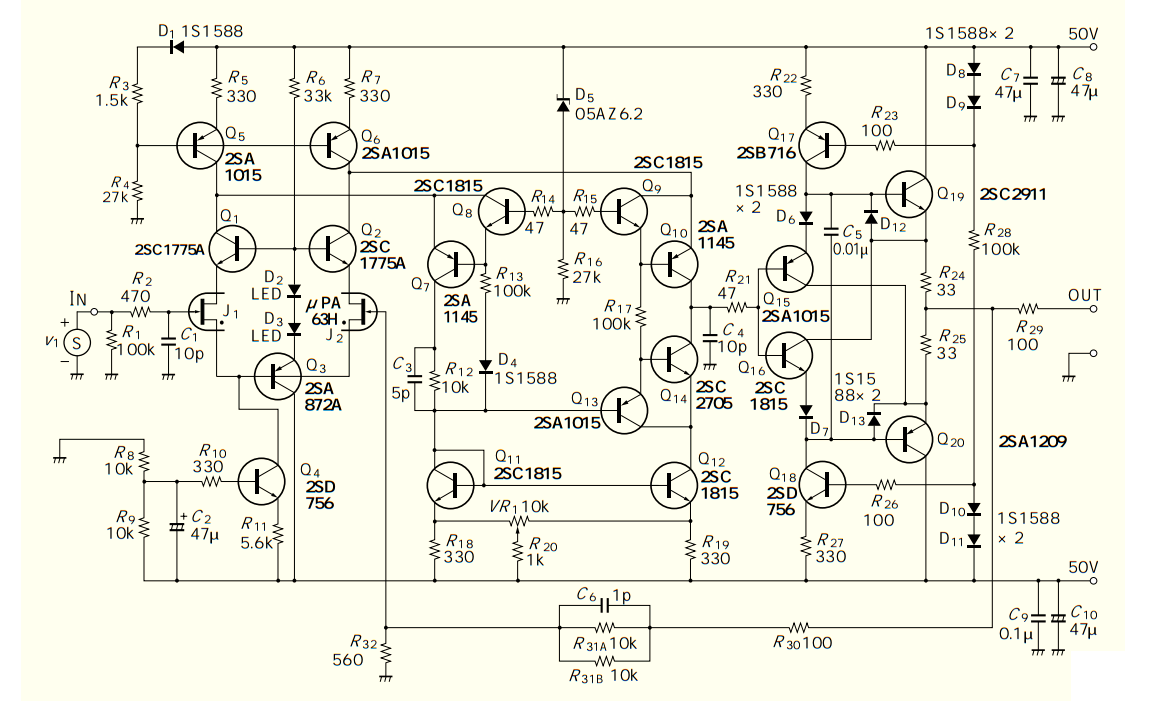
It’s a most impressive schematic!
I have had interest in the DB for a no loop feedback design. The pcb’s were made but I haven’t built it yet. Thanks to this thread I’ve been reminded!
TGM11 - no GNFB - inspired by Steven Dunlap 'KRILL'
And you make your own solder flux ! - an impressive range of projects on your blog, I sit in your shadow 🙂
Last edited:

If you don’t want thermal runaway, all 4 devices in diamond should be complements. In a practical discrete amp, Vbe differences can cause problems wherein one half of the DB can be off because one of the OP devices has a higher VBe than its input complement. This was a problem in the first sx-Amp from 2012. I added 150 ohm degeneration resistors and it was solved. I’ve stuck with this for all my subsequent CFA designs because it’s pretty robust and the offsets and drift are very low - eg drift over 30C < 10 mV measured at amp O/P so input referred it’s about 500 uV total or c. 15 uV/C. Offsets are almost always under 200 mV measured at amp output before dialing it out - that’s without selected transistors.
In IC’s they get around this problem by sizing the chip areas for the DB input and output devices differently - you don’t really want to add any more degeneration other than that afforded by ‘re.
(Important point: I run both input and output stage of the DB at 1 mA so the degeneration is c. 150 mV or about 25% of Vbe) YMMV.
Last edited:
Please stop calling this circuit diamond buffer. Baker diamond circuit is the modulator, not the follower.
Follower was invented by Seening Yee
Interesting that neither Seening Yee nor the patent examiner, cited Baker's 1963 paper in the References section.
Can we consider it as belonging to the diamond buffer family ?
It's a buffer, but in my opinion we can not consider it as belonging to the "Diamond Buffer" family.


Headphone Amp - WNA MKII versus WNA MKIII
Attachments


Last edited:
Lm6171 internal schematic diagram
In your first picture.
The input stage is an H-bridge, using two Diamonds and the output stage looks like a Diamond EF3 variant.
There are so many threads here about diamond buffers, different versions and implementations. Some have been built and tested many times, others maybe not even once. I have been thinking about starting a thread like this as well, but more with the intention of creating something like a "Diamond Buffer compendium" in a collective effort. A proper systematisation/overview and naming scheme would be helpful, so would be comparable simulations and measurements. A free document everyone could reference when talking about diamond buffers and simulation files to go along with it. But I guess diamond buffers are far too boring to get any of the analog gurus here involved in such an effort.

This driverstage (from R24, C4 to out) looks like good for me.
What are the BC, BD comparative types for SA, SB, SC, SD BJTs?
Is 1S1588 similar with 1N4148?
Are D8,9 or D10,11 replaceable with LEDs (green or read)?
What are the BC, BD comparative types for SA, SB, SC, SD BJTs?
Is 1S1588 similar with 1N4148?
Are D8,9 or D10,11 replaceable with LEDs (green or read)?
Last edited:
with the intention of creating something like a "Diamond Buffer compendium" in a collective effort. A proper systematisation/overview and naming scheme would be helpful, so would be comparable simulations and measurements. A free document everyone could reference when talking about diamond buffers and simulation files to go along with it. But I guess diamond buffers are far too boring to get any of the analog gurus here involved in such an effort.
Thats a good idea that I can support, but when it comes to the "analog gurus" I'm not sure who you actually are talking about, I think that you have to name them.
This driverstage (from R24, C4 to out) looks like good for me.
What are the BC, BD comparative types for SA, SB, SC, SD BJTs?
Is 1S1588 similar with 1N4148?
Are D8,9 or D10,11 replaceable with LEDs (green or read)?
Firs off all: the "Diamond" starts after R21.
C4 is a CComp for the amp and has notting to do with the "Diamond".
If this or that component can be replased by this or that component has absultally notting to do about how the "Diamond" works.
The diodes you are mentioning are simply making a voltage drop to set the the current source / sink standing current together with Q17 and Q19 and R22 and R27 at the in inputstage of the "Diamond"
They can be replaced by LED's, but it's always a good idea to use diodes that has close to the same "tempco" as the trasistors or even better to use diode connected transistors.
Stein
Thats a good idea that I can support, but when it comes to the "analog gurus" I'm not sure who you actually are talking about, I think that you have to name them.
Firs off all: the "Diamond" starts after R21.
C4 is a CComp for the amp and has notting to do with the "Diamond".
If this or that component can be replased by this or that component has absultally notting to do about how the "Diamond" works.
The diodes you are mentioning are simply making a voltage drop to set the the current source / sink standing current together with Q17 and Q19 and R22 and R27 at the in inputstage of the "Diamond"
I know that, this was only an approximate location information - my mistake!
They can be replaced by LED's, but it's always a good idea to use diodes that has close to the same "tempco" as the trasistors or even better to use diode connected transistors.
Stein
Or using Constant Current Diodes - CDR? This could save everything around Q17, Q18.
Linear Systems J500 Series
Semitec CRD
Or LM334 or similar LM334 data sheet, product information and support | TI.com
- Home
- Amplifiers
- Solid State
- Diamond Buffer variations