I still want to press on this, DLH is such an elegant design that I think we should minimize any reliability risk.
Looking into your comparison with PLH on dissipation, and your figure of 135mW, I believe your calculation is only based on idle status. You mentioned that the bias of the front end is 12.5mA, so I believe you use this as base and estimate the effective resistance between the 2 wipers of the 2 Pots. This comes close to 135mW? In such case, this is only as good as the amp is at idle. When it plays music, the 4700uF bootstrap capacitor will have an AC current flowing thru. This AC current will then flow thru the effective resistance between the 2 wipers of the Pots and then to +V, which is effectively GND in AC terms. I believe this AC current will be significant bigger than 12.5mA. I do not know how to calculate, but if you can help to check if you can read the current thru the 4700uF from your LTSpice model, say at 1W/8 Ohm output level. If we check that and still find the dissipation is OK, then I feel good. My guess is that it will not.

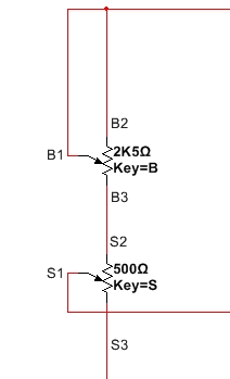
Taking the following scheme of reference, the maximum power dissipation in each of the trimpots will be a function of several parameters. Some of these parameters are: Vgs of both mosfets, position of S1 and of B1, tolerance in the value of the total resistance of the trimpots, tolerance of the resistance of 390 ohm, etc.
In my actual circuit, the total resistance of the two trimpots is 864 ohms (between B1 - S3), for a bias current of about 1.4 A. From now on, tolerances will be neglected (for a simpler analysis). Between B1 and B3 there are only 364 ohms.
That portion between B1 and B3 could dissipate a maximum power of Pb1b3 = ( 364 / 2500 ) x 0.5 W = 0.0728 W.
S1 was set for the lowest THD. For this function, the resistance between S1 and S3 is about 1 / 3 of the total between S2 and S3. This is 288 ohms for Rs1s3. Thus, Rs2s1 is 212 ohms. The portion between S1 and S3 could dissipate a maximum power of Ps1s3 = ( 288 / 500 ) x 0.5 W = 0.288 W. The portion between S2 and S1 could dissipate a maximum power of Ps2s1 = ( 212 / 500 ) x 0.5 W = 0.212 W.
The average voltage between B1 and S1 is 7.28 V, with peaks reaching + 15.12 V and - 0.56 V. This voltage was measured with input sine signal of 1 KHz and 2 V RMS and with output load of 2 ohms.
The average voltage between S1 and S3 is 3.52 V, with peaks reaching + 3.98 V and + 3.00 V.
The average power (without applying signal) on S1 and S3 is 0.043 W. The RMS power (applying signal) on S1 and S3 is 0.052 W.
As you can see, the 500 ohm trimpot can handle the situation with ease, since 0.288 W > 0.052 W.
The average power (without applying signal) on B1 and S1 is 0.092 W. The RMS power (applying signal) on B1 and S1 is 0.285 W.
Of those 0.285 W, S1 - S2 dissipate one part and B1 - B3 dissipate the other part. The resistance B1 - S1 is 576 ohms, of which 212 ohms correspond to the lower trimpot. The other 364 ohms correspond to the upper trimpot.
Of those 0.285 W, about 0.105 W are developed between S1 - S2. As can be seen, it is tolerated by the capacity of the lower trimpot, since 0.212 W > 0.105 W.
Of those 0.285 W, about 0.180 W are developed between B1 - B3. This would exceed the capacity of the upper trimpot, since 0.0728 W < 0.180W. If this situation occurs, the solution is to use a trimpot of lower value for the upper one. For example, if you replace the 2K5 trimpot with a 1K of similar power dissipation, now the 364 ohm portion of the new trimpot will tolerate 0.182 W.
I always try to make the adjustments to be finally in the middle of the trimpot track. It is not always possible.
Another thing to be contemplated is that the amplifier will never be in its maximum excursion condition for long periods.
I first put 2K5, in case the Vgs fall to the minimum expected. In that way, it is more difficult to ruin the mosfets by overcurrent.
We can then replace the trimpot of 2k5 with fixed metal film resistors, once the desired bias is set.
Regards
Last edited:
When S1 is fully set in SE, the dissipation situation may be more favorable.
In the PLH paper, this is not explained in detail. I hope this serves to clarify it.
Regards
In the PLH paper, this is not explained in detail. I hope this serves to clarify it.
Regards
Last edited:
By the way, I just notice that your feedback network carries a very low resistance, 100R and 56R only. This low resistance path to GND might save the Pots as this might shunt away a lot of current. Why do you choose such a low resistance?
The reasons for this have already been explained in this thread. Reference: DLH Amplifier: The trilogy with PLH and JLH amps
Regards
Last edited:
Some interesting facts:
DLH ( Output load = 2 ohms ):
Open loop gain = 45 dB approx.
Closed loop gain = 8.9 dB approx.
Feedback = 36.1 dB approx.
JLH:
Open loop gain = 55 dB approx.
Closed loop gain = 22 dB approx.
Feedback = 33 dB approx.
PLH:
Open loop gain = 27 dB approx.
Closed loop gain = 17 dB approx.
Feedback = 10 dB approx.
Regards
Last edited:
S1 was set for the lowest THD. For this function, the resistance between S1 and S3 is about 1 / 3 of the total between S2 and S3. This is 288 ohms for Rs1s3. Thus, Rs2s1 is 212 ohms. The portion between S1 and S3 could dissipate a maximum power of Ps1s3 = ( 288 / 500 ) x 0.5 W = 0.288 W. The portion between S2 and S1 could dissipate a maximum power of Ps2s1 = ( 212 / 500 ) x 0.5 W = 0.212 W.
Replace by:
S1 was set for the lowest THD. For this function, the resistance between S1 and S3 is about 1 / 3 of the total between B1 and S3. This is 288 ohms for Rs1s3. Thus, Rs2s1 is 212 ohms. The portion between S1 and S3 could dissipate a maximum power of Ps1s3 = ( 288 / 500 ) x 0.5 W = 0.288 W. The portion between S2 and S1 could dissipate a maximum power of Ps2s1 = ( 212 / 500 ) x 0.5 W = 0.212 W.
Sorry
Thanks Diego for the very detailed calculations. The voltage and resistance figures are very helpful in understanding the dynamics. Yes you are right these pots should stand fine.
I might need a bit more gain than 8.9dB so I will need to boost up the 100R a bit, maybe to 200R to get about 4dB more.
I might need a bit more gain than 8.9dB so I will need to boost up the 100R a bit, maybe to 200R to get about 4dB more.
It is quite possible that increasing the closed loop gain will worsen the quality parameters. You would have to simulate the changes.
It is not a very flexible circuit ...
It was not very easy to find the optimum operating point ...
Regards
It is not a very flexible circuit ...
It was not very easy to find the optimum operating point ...
Regards
Last edited:
The clipping is asymmetrical. Anyway, if it is used for what was designed, this should not be a problem to worry about.
Diegomj,
could you add the post links to the latest version?
And maybe also to different implementations and/or PCB layouts etc?.
could you add the post links to the latest version?
And maybe also to different implementations and/or PCB layouts etc?.
I think this is the latest layout that Gaborbela made based on my layout that is currently playing. An input RFI filter was added. I think a topside component map/silkscreen would be very useful to have to go with this layout. If someone could volunteer to make that, it would be appreciated.
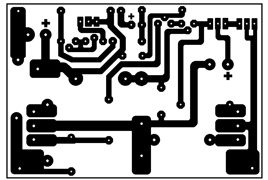


I just noticed an error in my layout - but apparently it was not big enough to keep the amp from working superbly well. I put the 390R after the 220R when it should have been before (on the BJT side). If you leave out the gate stopper 220R (jumper with solid wire) per Diegomj's original schematic then it doesn't matter. Thiago's layout is correct.


I think that looks good Gaborbela.
@Thiago, that looks beautiful, as always from you. Does the board extend over the top of the MOSFETs to provide screw hole mounting for PCB with heatsink screw, or is the outline the smaller rectangle?
@Thiago, that looks beautiful, as always from you. Does the board extend over the top of the MOSFETs to provide screw hole mounting for PCB with heatsink screw, or is the outline the smaller rectangle?


- Home
- Amplifiers
- Solid State
- DLH Amplifier: The trilogy with PLH and JLH amps