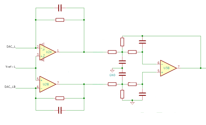
This is the first stage from DAC chip, it has 2 opamps buffer before outputIf your dac is like the schematic, then the output stage is not ideal. The output stage in the schematic is designed to be very low cost more than anything else.
The schematic @muducu posted is proper for this type of dac chip. I will copy it again here:
Also, attached below is an old ESS application note on various things including output stages.
You may notice that all the proper output stages do not have any resistors between the outputs of the dac chip and inputs to the first opamps. Having a circuit with resistors there is a clue that the design is most likely not very good.
Attachments
trungdtmc wrote:"This is the first stage from DAC chip, it has 2 opamps buffer before output"
So the schematic presented before is not that of the device...
... which surprises me a little in view of the price offered for this DAC.
A photo of the complete PCB would allow you to know a little more.
Generally, we find almost the same pattern in the devices offered on Chinese resale sites.
This is full pcb, i line one channel to easy follow. The schematic i posted that i found in this thread and post to compare with my DAC.trungdtmc wrote:"This is the first stage from DAC chip, it has 2 opamps buffer before output"
So the schematic presented before is not that of the device...
... which surprises me a little in view of the price offered for this DAC.
A photo of the complete PCB would allow you to know a little more.
Generally, we find almost the same pattern in the devices offered on Chinese resale sites.
2 relays to on off bypass 2 buffer opamps
Hi,
I would say from the view of this PCB:
"Why make it simple when you can make it complicated ?"
🙄
An excellent simplified and efficient diagram had been published on the site ->
View attachment 1132816
I invite all those who are concerned to follow it, including Chinese manufacturers... 😉
I would say from the view of this PCB:
"Why make it simple when you can make it complicated ?"
🙄
An excellent simplified and efficient diagram had been published on the site ->
View attachment 1132816
I invite all those who are concerned to follow it, including Chinese manufacturers... 😉
Last edited:
PS: you will find that here it is a low pass filter which further reduces the HF 'residues' of the analog output signal (good) with its resistor which also protects the output OPAMP (good) unlike a high pass filter (less useful even useless here) which adds a capacitor in the signal path (worse) and does not protect the output OPAMP (not good).
The latter could be useful to protect the speakers from a 'PLOC !' but generally the device to which it is connected already has a filter of this type at its input.
NB: having two high pass filters in series (so in the DAC and in the amp) degrades the signal even more but also larger phase rotations 😒
Last edited:
oopsHi,
I would say from the view of this PCB:
"Why make it simple when you can make it complicated ?"
🙄
An excellent simplified and efficient diagram had been published on the site ->
View attachment 1132816
I invite all those who are concerned to follow it, including Chinese manufacturers... 😉
do you mean thereView attachment 1132823
PS: you will find that here it is a low pass filter which further reduces the HF 'residues' of the analog output signal (good) with its resistor which also protects the output OPAMP (good) unlike a high pass filter (less useful even useless here) which adds a capacitor in the signal path (worse) and does not protect the output OPAMP (not good).
The latter could be useful to protect the speakers from a 'PLOC !' but generally the device to which it is connected already has a filter of this type at its input.
NB: having two high pass filters in series (so in the DAC and in the amp) degrades the signal even more but also larger phase rotations 😒
//oh i was mistaken, my DAC does not i/V stage, the first stage is Diffrential convert SE
Last edited:
In fact I think the circuit on the PCB looks like this ->
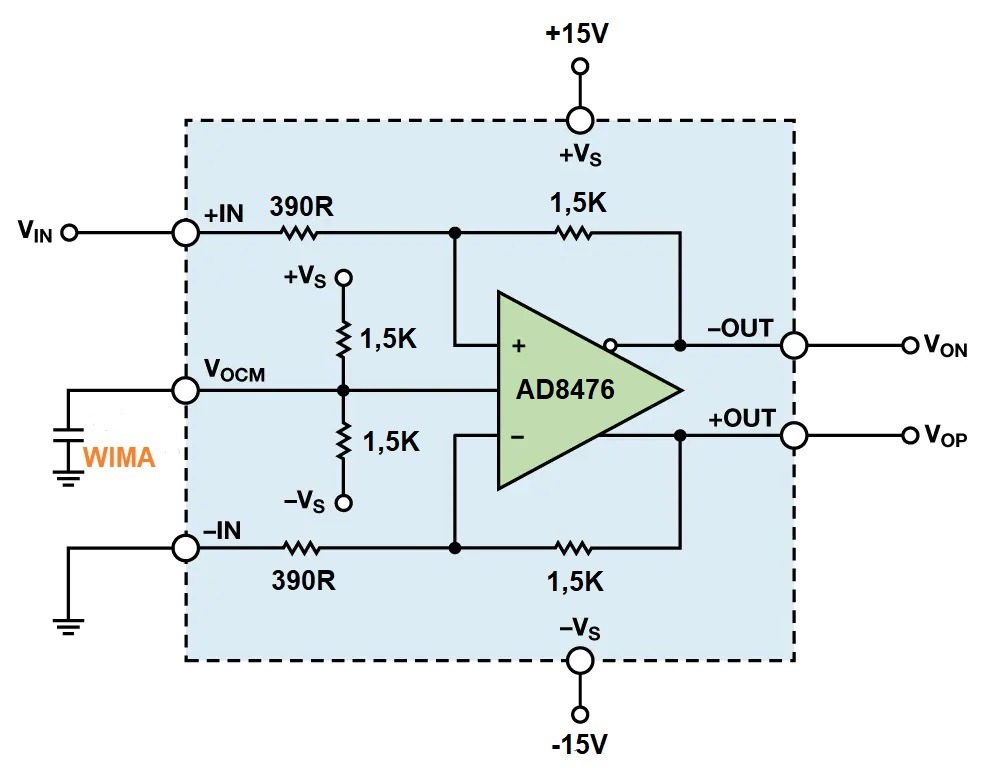
but it involves the use of a dedicated OPAMP but on this diagram there is only one channel while your DAC has two.
So they did a kind of 'tinkering' (virtual ground usage) with a usual double OPAMP to get the two channels...
...that's a bit like the diagram you showed us, but that implies the presence of components (resistors) under the PCB, is that the case ?
Last edited:
no, bottom side only for wiring, does not have any componentsIn fact I think the circuit on the PCB looks like this ->
View attachment 1132845
but it involves the use of a dedicated OPAMP but on this diagram there is only one channel while your DAC has two.
So they did a kind of 'tinkering' (virtual ground usage) with a usual double OPAMP to get the two channels...
...that's a bit like the diagram you showed us, but that implies the presence of components (resistors) under the PCB, is that the case ?
Here's what I would recommend to do:
1. get a copy of the dac chip datasheet and examine the pinouts. Most ESS datasheets can now be downloaded from Mouser.
2. get or make a needle tip probe for your DVM
3. turn off the dac power and using DVM continuity measurements when necessary, start tracing out a schematic from the dac chip analog outputs to the opamps, then from there to the analog outputs of the dac box.
4. analyze the schematic you just produced to understand how the circuit works. With a two-layer board its easy. Helps if the DVM has a beeper function for continuity testing.
Most likely it will turn out that the circuit in the dac is pretty close to one of the schematics recently posted in this thread. If not, we should still be able to analyze it pretty well.
i measure direct where the DAC output and the signal is rolling down right here, so problem truely from the internal filter
Hi trungdtmc,
I think your measurements must be 'distorted' because the passive components (resistors and capacitors) of the analog audio processing circuit located just behind the output pins of the DAC chip would have to be isolated to be certain, otherwise these ( which form the high-pass filter) always act, even if you measure upstream of them, either directly to the DAC output pins (2, 3, 8 and 9).
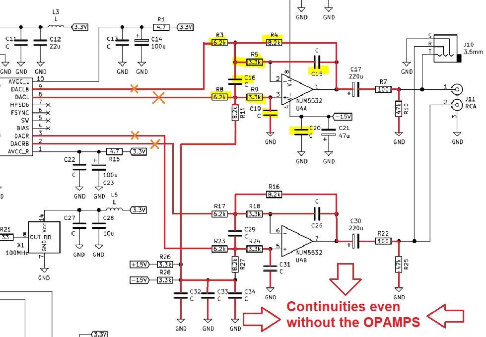
I think your measurements must be 'distorted' because the passive components (resistors and capacitors) of the analog audio processing circuit located just behind the output pins of the DAC chip would have to be isolated to be certain, otherwise these ( which form the high-pass filter) always act, even if you measure upstream of them, either directly to the DAC output pins (2, 3, 8 and 9).
Last edited:
Direct mesurement like this ->
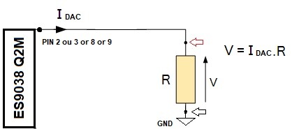
Once the measurements have been made to obtain the real shape of the output signal, I think you should use SPICE to model with the diagram and the value of the components found on your PCB to know which component(s) to act on. rectify analog output signal 😉
I remain convinced that the value of the red WIMAcapacitors are those which influence the appearance of the output signal... 🙄
Indeed we must not forget that the DAC outputs have their own internal impedance or they come to form a natural low pass when they encounter a capacitor in parallel on their path ->
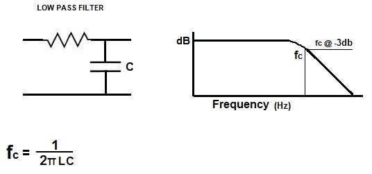
Last edited:
ESS dacs have several built-in filters. The default one is linear phase and should not affect the audio band, although the 'slow' filters will do so a little. IME the slow filters do sound rolled off some at HF. If that's the problem, the only fix is to go into the dac registers via I2C bus and change the filter to a different setting.
Hi Markw4,
Correct, it is a solution if it does not come from the audio circuit...
As such Markw4, what type of filter do you use with this chip out of the 7 available ?
(NB: the one that you think gives the best rendering)
Have you tried installable filters in FOOBAR for example ?
Or which one do you use ?
It would be interesting to elaborate on the settings in FOOBAR as well 😀
During normal operation oversampling dacs upsample the digital audio data. Upsampling commonly is implemented by zero stuffing followed by interpolation filtering. If that process takes place inside the dac chip then filtering would need to occur there too.
The filter I would use is the filter control register default, the linear phase one. Tried them all at one time and thought that one was best so long as the output stage and other parts of the dac hardware design were good.
However, ESS dacs can also accept externally upsampled and interpolated audio, although IIRC that option limits the maximum audio sample rate somewhat. To enable that feature also requires accessing the I2C registers to disable internal oversampling. At the same time if the dac is fully synchronous then the internal ASRC can be disabled by setting DPLL_Bandwidth to zero.
Taking over control of the dac registers also may imply taking control away from the MCU in the dac so that things like the display, volume control, input selection, etc., might be disabled, at least temporarily. For the dac board mostly used in this thread the MCU was pretty tolerant of losing I2C contact with the dac chip for a period of time, then reconnecting without crashing or other unwanted behavior. It might even be possible to seize the I2C bus briefly without disconnecting the normal MCU. Depends.
Regarding foobar, I normally leave it at full volume and with no DSP enabled. In some cases it may help to turn down the foobar volume slider down a few dB to help prevent intersample overs in the dac. For drivers, I either set foobar to use WASAPI Exclusive Mode or else ASIO. If using ASIO its important to check that Windows does not designate the dac as the "Default Sound Device" nor as the "Default Communication Device" or else Windows will feel free to resample your audio stream without warning and it will do so at something less than a very high fidelity quality level.
Last edited:
Ok Markw4.
Wich linear phase filter do you use ?
1> Linear phase, Slow roll-off


2> Linear phase, Fast roll-off


Wich linear phase filter do you use ?
1> Linear phase, Slow roll-off
2> Linear phase, Fast roll-off
Sorry. Its been awhile since I worked with this chip. To the best of my recollection it was the default filter, which I thought was linear phase. Oh, well.
Pic shows default filter for this chip is apodizing. If it wasn't that one it must have been linear phase fast:
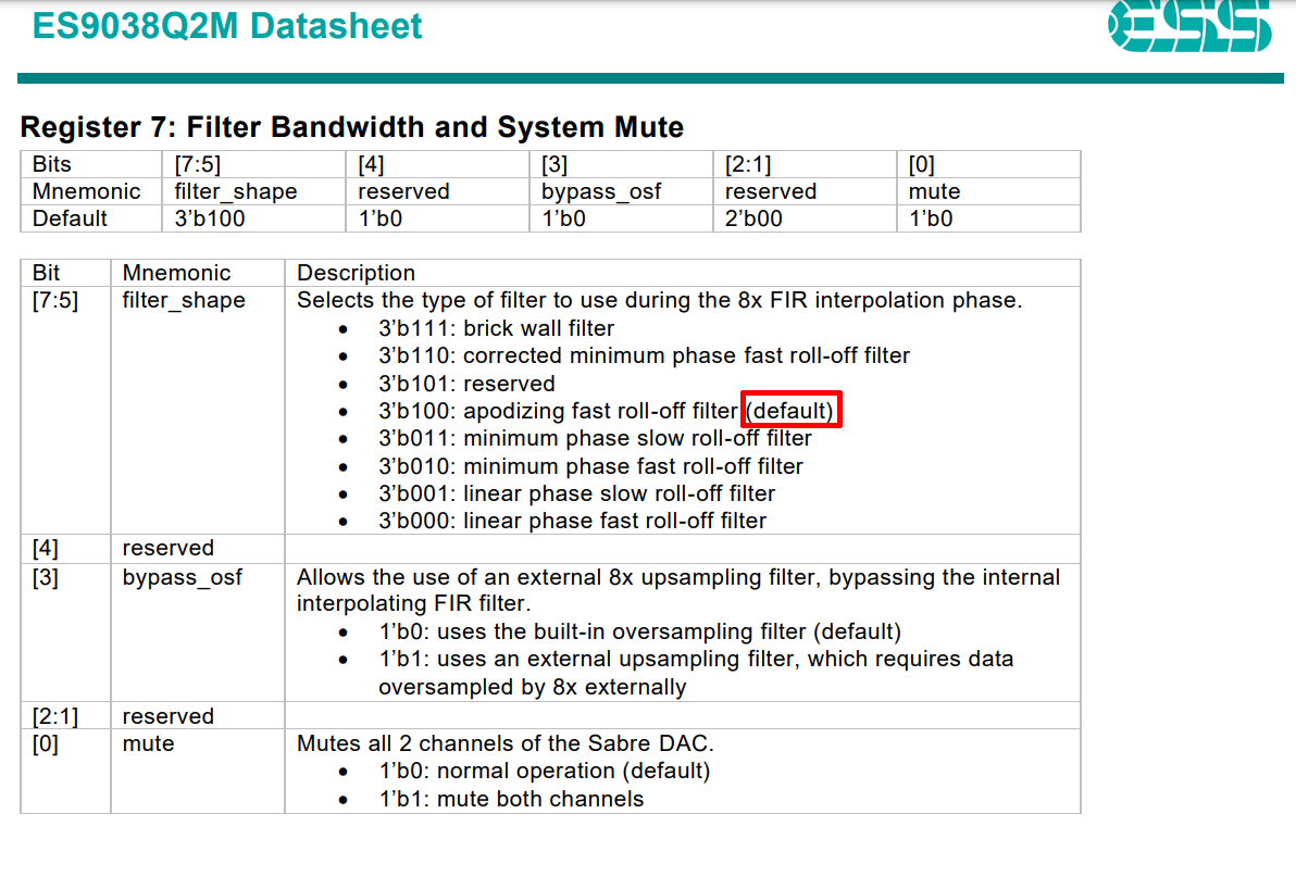
Pic shows default filter for this chip is apodizing. If it wasn't that one it must have been linear phase fast:
- Home
- Source & Line
- Digital Line Level
- ES9038Q2M Board