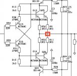
Sorry I don't know on top of my head, I added parts as I went, and going through my own pcb design. BTW I think there is a missing node on the schematic ver 1.2, see image.
SB
Somehow when I transferred schematic from ExpressSCH to jpg that nod was lost. Here is the schematic again.
Attachments
Hello,
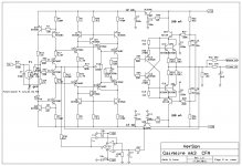
I simulated the output stage of this GainWire and I want to say that is a elegant and simply form to reduce the distorsion from output transistors. I want to ask you something.Is this a form of cascoding (bootstrap cascode), in order to reduce the distorsion from Early Effect? If I am right, this form reduces very much overall THD especialy Intermodulation Distorsion.
I simulated the output stage of this GainWire and I want to say that is a elegant and simply form to reduce the distorsion from output transistors. I want to ask you something.Is this a form of cascoding (bootstrap cascode), in order to reduce the distorsion from Early Effect? If I am right, this form reduces very much overall THD especialy Intermodulation Distorsion.
Hello,
I simulated the output stage of this GainWire and I want to say that is a elegant and simply form to reduce the distorsion from output transistors. I want to ask you something.Is this a form of cascoding (bootstrap cascode), in order to reduce the distorsion from Early Effect? If I am right, this form reduces very much overall THD especialy Intermodulation Distorsion.
Yes, you are exactly correct, the bootstrap cascode keeps quite constant voltage on output transistors. Down side of this OPS, it can't drive close to the power supply voltage, but here in preamp it's not so important.
Here in this CFA designed I could use simpler OPS as distortion will be decreased by quite high NFB, but I kept the same OPS I used in my first GainWire preamp working with no GNFB. Second GainWire mk2 used the same OPS and has possibility to work in CFA and non GNFB. This one has lowest distortion and better headphones drive possibility.
Dadod,
This circuit is quite amazing - the predicted distortion is essentially immeasurable. Is it true that qnty 4 BC550/560's provide all the drive current for the output? There are two TO126's BD's but it looks like all current still had to flow through the little TO-92's. What is the purpose of the BD139/140 situated backwards with base connected to outputs?
This circuit is quite amazing - the predicted distortion is essentially immeasurable. Is it true that qnty 4 BC550/560's provide all the drive current for the output? There are two TO126's BD's but it looks like all current still had to flow through the little TO-92's. What is the purpose of the BD139/140 situated backwards with base connected to outputs?
use LSK170ADamir,why you are choosing this demon transistor that is out of production?
the lower Idss of the A grade will better suit the CCS duty in the regulator.
Since the jFET has Vbe+Vf across it, you will find that other slightly higher "Vpinchoff" voltage jFETs will work in this circuit. Aim for Vpinchoff <1V
also, for folks that don't have stock waiting to be used, might there be cheaper, more easily available jfets that make better current sources?
some experts around here have said large geometry (low noise, high gm, high capacitance) devices are not the best choice for current sources anyway.
mlloyd1
some experts around here have said large geometry (low noise, high gm, high capacitance) devices are not the best choice for current sources anyway.
mlloyd1
use LSK170A
the lower Idss of the A grade will better suit the CCS duty in the regulator.
Since the jFET has Vbe+Vf across it, you will find that other slightly higher "Vpinchoff" voltage jFETs will work in this circuit. Aim for Vpinchoff <1V
Would J113 work?
It might if you find one with low Vgs(off) ("Vpinchoff") voltage, lower then -1.5V.
")

It might if you find one with low Vgs(off) ("Vpinchoff") voltage, lower then -1.5V.
I am new with measuring FETs - can you show link to simple rig to measure vgs at home?
Thanks.
Here's Borbely's article in two parts
OK, Andrew have sent those very nice jfet Borbely's articles.
As Idss is correlated with Vgs(off) for the same jfet type, it's quite simple to check for Idss, short the gate to the source and connect the drain to the 15 V via 7k5 resistor(source to - and resistor to +, this is similar condition in which it's used in the shunt) and low Idss (look the J113 data sheet).
This is preorder list:
platon.rado ----- 1
mlloyd1--------- 2
xrk971-----------1
reaper996--------1
Arthur-----------2
Tonza75-----------2
schillg11---------1
vac231-----------2
zrxshack----------1
erik777-----------1
pinnocchio--------1 changed to Alger_emi
Everybody answered my PMs and paid except zrxshack----------1 and erik777-----------1.
Please send me PM with yours PayPal email addresses if you are still interested.
BR Damir
Here's Borbely's article in two parts
Thank you, Andrew.
- Home
- Amplifiers
- Solid State
- GainWire Mk3 CFA pre/phone amp with very low distortion